 | –≠–ª–µ–∫—Ç—Ä–æ–Ω–Ω—ã–π –∫–æ–º–ø–æ–Ω–µ–Ω—Ç: NM24C16U | –°–∫–∞—á–∞—Ç—å:  PDF PDF  ZIP ZIP |

1
www.fairchildsemi.com
NM24C16U/17U Rev. B.1
NM24C16U/NM24C17U ≠ 16K-Bit Serial EEPROM 2-Wire Bus Interface
August 1999
© 1999 Fairchild Semiconductor Corporation
NM24C16U/NM24C17U
16K-Bit Serial EEPROM
2-Wire Bus Interface
General Description
The NM24C16U/17U devices are 16K (16,384) bit serial interface
CMOS EEPROMs (Electrically Erasable Programmable Read-
Only Memory). These devices fully conform to the Standard I
2
CTM
2-wire protocol which uses Clock (SCL) and Data I/O (SDA) pins
to synchronously clock data between the "master" (for example a
microprocessor) and the "slave" (the EEPROM device). In addi-
tion, the serial interface allows a minimal pin count packaging
designed to simplify PC board layout requirements and offers the
designer a variety of low voltage and low power options.
NM24C17U incorporates a hardware "Write Protect" feature, by
which, the upper half of the memory can be disabled against
programming by connecting the WP pin to V
CC
. This section of
memory then effectively becomes a ROM (Read-Only Memory)
and can no longer be programmed as long as WP pin is connected
to V
CC
.
Fairchild EEPROMs are designed and tested for applications requir-
ing high endurance, high reliability and low power consumption for a
continuously reliable non-volatile solution for all markets.
Block Diagram
Functions
I
I
2
CTM compatible interface
I
4,096 bits organized as 512 x 8
I
Extended 2.7V ≠ 5.5V operating voltage
I
100 KHz or 400 KHz operation
I
Self timed programming cycle (6ms typical)
I
"Programming complete" indicated by ACK polling
I
NM24C17U: Memory "Upper Block" Write Protect pin
Features
I
The I
2
CTM interface allows the smallest I/O pincount of any
EEPROM interface
I
16 byte page write mode to minimize total write time per byte
I
Typical 200
µ
A active current (I
CCA
)
I
Typical 1
µ
A standby current (I
SB
) for "L" devices and 0.1
µ
A
standby current for "LZ" devices
I
Endurance: Up to 1,000,000 data changes
I
Data retention greater than 40 years
H.V. GENERATION
TIMING &CONTROL
E2PROM
ARRAY
YDEC
DATA REGISTER
XDEC
CONTROL
LOGIC
WORD
ADDRESS
COUNTER
SLAVE ADDRESS
REGISTER &
COMPARATOR
START
STOP
LOGIC
CK
DIN
R/W
SDA
SCL
VSS
WP
VCC
DOUT
DS800010-1
I
2
CTM is a registered trademark of Philips Electronics N.V.
2
www.fairchildsemi.com
NM24C16U/17U Rev. B.1
NM24C16U/NM24C17U ≠ 16K-Bit Serial EEPROM 2-Wire Bus Interface
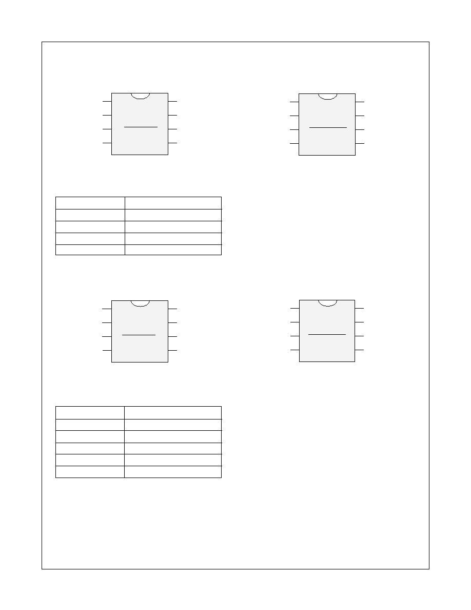
Connection Diagrams
Dual-In-Line Package (N),
8-Pin SO Package (M8)
Top View
See Package Number N08E, M08A and MTC08
Pin Names
V
SS
Ground
SDA
Serial Data I/O
SCL
Serial Clock Input
NC
No Connection
V
CC
Power Supply
Dual-In-Line Package (N),
8-Pin SO Package (M8)
Top View
See Package Number N08E, M08A and MTC08
Pin Names
V
SS
Ground
SDA
Serial Data I/O
SCL
Serial Clock input
WP
Write Protect
V
CC
Power Supply
NC
No Connection
NC
NC
NC
VSS
VCC
WP
SCL
SDA
8
7
6
5
1
2
3
4
NC
NC
NC
VSS
VCC
NC
SCL
SDA
8
7
6
5
1
2
3
4
NM24C16U
NM24C17U
DS800010-2
DS800010-4
8-Pin TSSOP Package (MT8)
Rotated Die (24C16UT)
NC
VCC
NC
NC
SCL
SDA
VSS
NC
8
7
6
5
1
2
3
4
DS800010-3
NM24C16UT
8-Pin TSSOP Package (MT8)
Rotated Die (24C17UT)
DS800010-5
WP
VCC
NC
NC
SCL
SDA
VSS
NC
8
7
6
5
1
2
3
4
NM24C17UT

3
www.fairchildsemi.com
NM24C16U/17U Rev. B.1
NM24C16U/NM24C17U ≠ 16K-Bit Serial EEPROM 2-Wire Bus Interface
Ordering Information
NM
24
C
XX
U
F
T
LZ
E
XX
Letter
Description
Package
N
8-pin DIP
M8
8-pin SOIC
MT8
8-pin TSSOP
Temp. Range
None
0 to 70
∞
C
V
-40 to +125
∞
C
E
-40 to +85
∞
C
Voltage Operating Range
Blank
4.5V to 5.5V
L
2.7V to 5.5V
LZ
2.7V to 5.5V and
<1
µ
A Standby Current
Blank
Normal Pin Out
T
Rotated Die Pin Out
SCL Clock Frequency
Blank
100KHz
F
400KHz
Ultralite
CS100UL Process
Density
16
16K
17
16K with Write Protect
C
CMOS Technology
W
Total Array Write Protect
Interface
24
IIC
NM
Fairchild Non-Volatile
Memory

4
www.fairchildsemi.com
NM24C16U/17U Rev. B.1
NM24C16U/NM24C17U ≠ 16K-Bit Serial EEPROM 2-Wire Bus Interface
Product Specifications
Absolute Maximum Ratings
Ambient Storage Temperature
≠65
∞
C to +150
∞
C
All Input or Output Voltages
with Respect to Ground
6.5V to ≠0.3V
Lead Temperature
(Soldering, 10 seconds)
+300
∞
C
ESD Rating
2000V min.
Operating Conditions
Ambient Operating Temperature
NM24C16U/17U
0
∞
C to +70
∞
C
NM24C16UE/17UE
-40
∞
C to +85
∞
C
NM24C16UV/17UV
-40
∞
C to +125
∞
C
Positive Power Supply
NM24C16U/17U
4.5V to 5.5V
NM24C16UL/17UL
2.7V to 5.5V
NM24C16ULZ/17ULZ
2.7V to 5.5V
Standard V
CC
(4.5V to 5.5V) DC Electrical Characteristics
Symbol
Parameter
Test Conditions
Limits
Units
Min
Typ
Max
(Note 1)
I
CCA
Active Power Supply Current
f
SCL
= 400 KHz
0.2
1.0
mA
f
SCL
= 100 KHz
I
SB
Standby Current
V
IN
= GND or V
CC
10
50
µ
A
I
LI
Input Leakage Current
V
IN
= GND to V
CC
0.1
1
µ
A
I
LO
Output Leakage Current
V
OUT
= GND to V
CC
0.1
1
µ
A
V
IL
Input Low Voltage
≠0.3
V
CC
x 0.3
V
V
IH
Input High Voltage
V
CC
x 0.7
V
CC
+ 0.5
V
V
OL
Output Low Voltage
I
OL
= 3 mA
0.4
V
Low V
CC
(2.7V to 5.5V) DC Electrical Characteristics
Symbol
Parameter
Test Conditions
Limits
Units
Min
Typ
Max
(Note 1)
I
CCA
Active Power Supply Current
f
SCL
= 400 KHz
0.2
1.0
mA
f
SCL
= 100 KHz
I
SB
Standby Current
V
IN
= GND
V
CC
= 2.7V - 4.5V
1
10
µ
A
or V
CC
V
CC
= 2.7V - 4.5V
0.1
1
µ
A
V
CC
= 4.5V - 5.5V
10
50
µ
A
I
LI
Input Leakage Current
V
IN
= GND to V
CC
0.1
1
µ
A
I
LO
Output Leakage Current
V
OUT
= GND to V
CC
0.1
1
µ
A
V
IL
Input Low Voltage
≠0.3
V
CC
x 0.3
V
V
IH
Input High Voltage
V
CC
x 0.7
V
CC
+ 0.5
V
V
OL
Output Low Voltage
I
OL
= 3 mA
0.4
V
Capacitance
T
A
= +25
∞
C, f = 100/400 KHz, V
CC
= 5V
(Note 2)
Symbol
Test
Conditions
Max
Units
C
I/O
Input/Output Capacitance (SDA)
V
I/O
= 0V
8
pF
C
IN
Input Capacitance (A0, A1, A2, SCL)
V
IN
= 0V
6
pF
Note 1: Typical values are T
A
= 25
∞
C and nominal supply voltage (5V).
Note 2: This parameter is periodically sampled and not 100% tested.

5
www.fairchildsemi.com
NM24C16U/17U Rev. B.1
NM24C16U/NM24C17U ≠ 16K-Bit Serial EEPROM 2-Wire Bus Interface
AC Conditions of Test
Input Pulse Levels
V
CC
x 0.1 to V
CC
x 0.9
Input Rise and Fall Times
10 ns
Input & Output Timing Levels
V
CC
x 0.5
Output Load
1 TTL Gate and C
L
= 100 pF
Read and Write Cycle Limits (Standard and Low V
CC
Range 2.7V - 5.5V)
Symbol
Parameter
100 KHz
400 KHz
Units
Min
Max
Min
Max
f
SCL
SCL Clock Frequency
100
400
KHz
T
I
Noise Suppression Time Constant at
SCL, SDA Inputs (Minimum V
IN
100
50
ns
Pulse width)
t
AA
SCL Low to SDA Data Out Valid
0.3
3.5
0.1
0.9
µ
s
t
BUF
Time the Bus Must Be Free before
4.7
1.3
µ
s
a New Transmission Can Start
t
HD:STA
Start Condition Hold Time
4.0
0.6
µ
s
t
LOW
Clock Low Period
4.7
1.5
µ
s
t
HIGH
Clock High Period
4.0
0.6
µ
s
t
SU:STA
Start Condition Setup Time
4.7
0.6
µ
s
(for a Repeated Start Condition)
t
HD:DAT
Data in Hold Time
0
0
µ
s
t
SU:DAT
Data in Setup Time
250
100
ns
t
R
SDA and SCL Rise Time
1
0.3
µ
s
t
F
SDA and SCL Fall Time
300
300
ns
t
SU:STO
Stop Condition Setup Time
4.7
0.6
µ
s
t
DH
Data Out Hold Time
300
50
ns
t
WR
Write Cycle Time - NM24C16U/17U
10
10
ms
(Note 3)
- NM24C16U/17UL, NM24C16U/17ULZ
15
15
Note 3: The write cycle time (t
WR
) is the time from a valid stop condition of a write sequence to the end of the internal erase/program cycle. During the write cycle, the
NM24C16U/17U bus interface circuits are disabled, SDA is allowed to remain high per the bus-level pull-up resistor, and the device does not respond to its slave address.