NM25C160 16K-Bit Serial CMOS EEPROM |(Serial Peripheral Interface (SPI) Synchronous Bus)
1
www.fairchildsemi.com
NM25C160 Rev. D.1
NM25C160 16K-Bit Serial CMOS EEPROM
(Serial Periphrial Interface (SPI) Synchronous Bus)
March 1999
© 1999 Fairchild Semiconductor Corporation
NM25C160
16K-Bit Serial CMOS EEPROM
(Serial Peripheral Interface (SPI) Synchronous Bus)
General Description
The NM25C160 is a 16,384-bit CMOS EEPROM with an SPI
compatible serial interface. The NM25C160 is designed for data
storage in applications requiring both non-volatile memory and in-
system data updates. This EEPROM is well suited for applications
using the 68HC11 series of microcontrollers that support the SPI
interface for high speed communication with peripheral devices
via a serial bus to reduce pin count. The NM25C160 is imple-
mented in Fairchild Semiconductor's floating gate CMOS process
that provides superior endurance and data retention.
The serial data transmission of this device requires four signal
lines to control the device operation: Chip Select (CS), Clock
(SCK), Data In (SI), and Serial Data Out (SO). All programming
cycles are completely self-timed and do not require an erase
before WRITE.
BLOCK WRITE protection is provided by programming the STA-
TUS REGISTER with one of four levels of write protection.
Additionally, separate WRITE enable and WRITE disable instruc-
tions are provided for data protection.
Hardware data protection is provided by the WP pin to protect
against inadvertent programming. The HOLD pin allows the serial
communication to be suspended without resetting the serial
sequence.
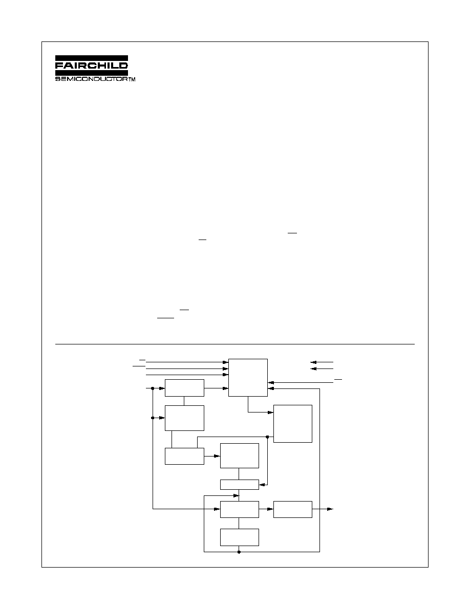
Block Diagram
Features
s
2.1 MHz clock rate @ 2.7V to 5.5V
s
16,384 bits organized as 2,048 x 8
s
Multiple chips on the same 3-wire bus with separate chip
select lines
s
Self-timed programming cycle
s
Simultaneous programming of 1 to 16 bytes at a time
s
Status register can be polled during programming to monitor
READY/BUSY
s
Write Protect (WP) pin and write disable instruction for both
hardware and software write protection
s
Block write protect feature to protect against accidental
writes
s
Endurance: 1,000,000 data changes
s
Data retention greater than 40 years
s
Packages available: 8-pin DIP, 8-pin SO, or 8-pin TSSOP
DS012402-1
Instruction
Decoder
Control Logic
and Clock
Generators
High Voltage
Generator
and
Program
Timer
Instruction
Register
Program
Enable
Data In/Out Register
8 Bits
Data Out
Buffer
Non-Volatile
Status Register
Decoder
1 of 2048
Address
Counter/
Register
EEPROM Array
16,384 Bits
(2048 x 8)
Read/Write Amps
CS
HOLD
SCK
V
CC
V
SS
V
PP
WP
SI
SO
2
www.fairchildsemi.com
NM25C160 Rev. D.1
NM25C160 16K-Bit Serial CMOS EEPROM
(Serial Periphrial Interface (SPI) Synchronous Bus)
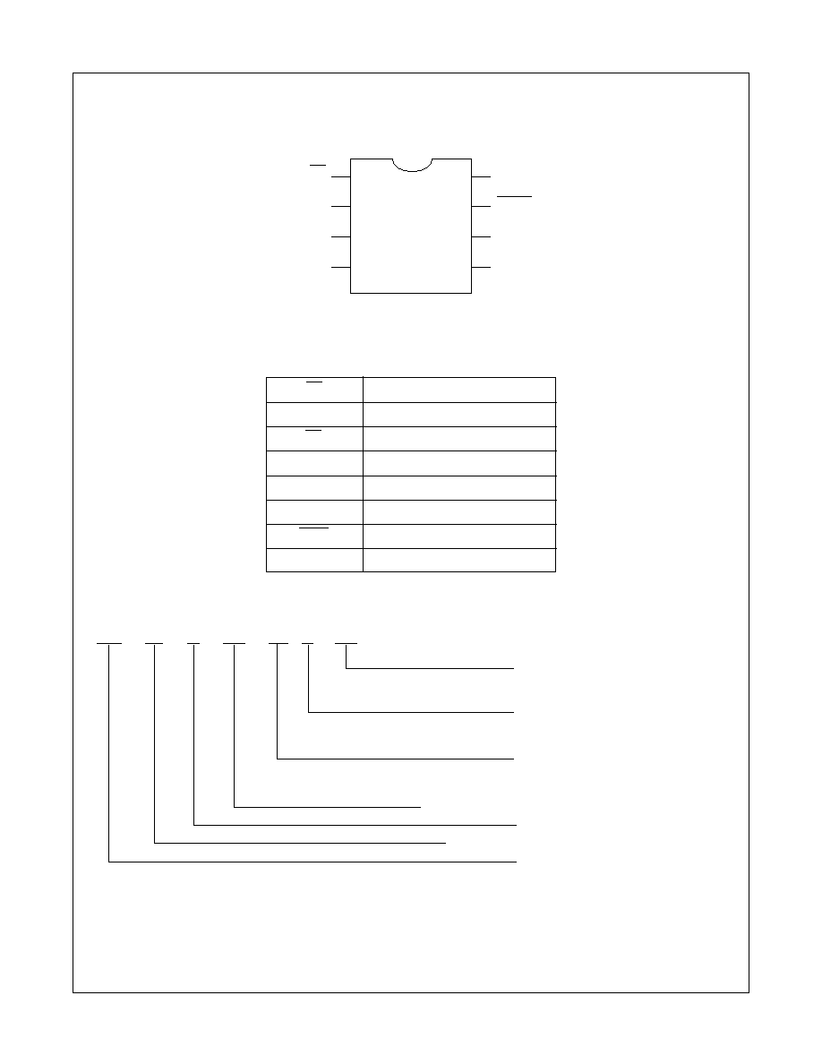
Connection Diagram
Dual-In-Line Package (N), SO Package (M8),
and TSSOP Package (MT8)
Top View
See Package Number N08E (N), M08A (M8), and MTC08 (MT8)
Pin Names
CS
Chip Select Input
SO
Serial Data Output
WP
Write Protect
V
SS
Ground
SI
Serial Data Input
SCK
Serial Clock Input
HOLD
Suspends Serial Data
V
CC
Power Supply
Ordering Information
NM
25
C
XX
LZ E
XX
Letter
Description
Package
N
8-pin DIP
M8
8-pin SO
MT8
8-pin TSSOP
Temp. Range
None
0 to 70
°
C
V
-40 to +125
°
C
E
-40 to +85
°
C
Voltage Operating Range
Blank
4.5V to 5.5V
L
2.7V to 4.5V
LZ
2.7V to 4.5V and
<1
µ
A Standby Current
Density/Mode
160
16K, mode 0
C
CMOS technology
Interface
25
SPI
NM
Fairchild Nonvolatile
Memory Prefix
CS
SO
WP
V
SS
V
CC
HOLD
SCK
SI
8
7
6
5
1
2
3
4
NM25C160
DS012402-2
3
www.fairchildsemi.com
NM25C160 Rev. D.1
NM25C160 16K-Bit Serial CMOS EEPROM
(Serial Periphrial Interface (SPI) Synchronous Bus)
Standard Voltage 4.5
V
CC
5.5V Specifications
Absolute Maximum Ratings
(Note 1)
Ambient Storage Temperature
-65
°
C to +150
°
C
All Input or Output Voltage with
Respect to Ground
+6.5V to -0.3V
Lead Temp. (Soldering, 10 sec.)
+300
°
C
ESD Rating
2000V
Operating Conditions
Ambient Operating Temperature
NM25C160
0
°
C to +70
°
C
NM25C160E
-40
°
C to +85
°
C
NM25C160V
-40
°
C to +125
°
C
Power Supply (V
CC
)
4.5V to 5.5V
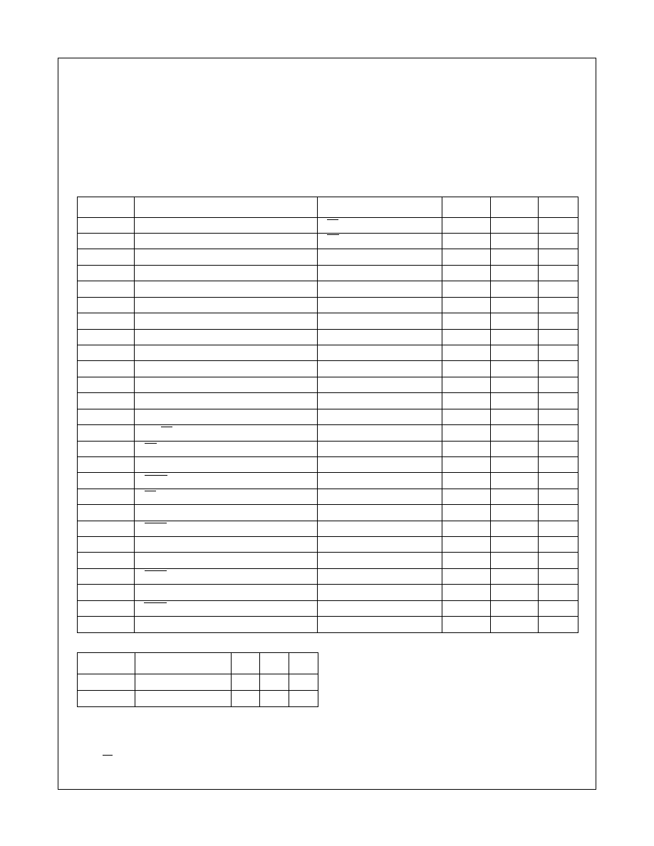
DC and AC Electrical Characteristics
4.5V
V
CC
5.5V (unless otherwise specified)
Symbol
Parameter
Conditions
Min
Max
Units
I
CC
Operating Current
CS = V
IL
3
mA
I
CCSB
Standby Current
CS = V
CC
50
µ
A
I
IL
Input Leakage
V
IN
= 0 to V
CC
-1
+1
µ
A
I
OL
Output Leakage
V
OUT
= GND to V
CC
-1
+1
µ
A
V
IL
CMOS Input Low Voltage
-0.3
V
CC
* 0.3
V
V
IH
CMOS Input High Voltage
0.7 * V
CC
V
CC
+ 0.3
V
V
OL
Output Low Voltage
I
OL
= 1.6 mA
0.4
V
V
OH
Output High Voltage
I
OH
= -0.8 mA
V
CC
- 0.8
V
f
OP
SCK Frequency
2.1
MHz
t
RI
Input Rise Time
2.0
µ
s
t
FI
Input Fall Time
2.0
µ
s
t
CLH
Clock High Time
(Note 2)
190
ns
t
CLL
Clock Low Time
(Note 2)
190
ns
t
CSH
Min CS High Time
(Note 3)
240
ns
t
CSS
CS Setup Time
240
ns
t
DIS
Data Setup Time
100
ns
t
HDS
HOLD Setup Time
90
ns
t
CSN
CS Hold Time
240
ns
t
DIN
Data Hold Time
100
ns
t
HDN
HOLD Hold Time
90
ns
t
PD
Output Delay
C
L
= 200 pF
240
ns
t
DH
Output Hold Time
0
ns
t
LZ
HOLD to Output Low Z
100
ns
t
DF
Output Disable Time
C
L
= 200 pF
240
ns
t
HZ
HOLD to Output High Z
100
ns
t
WP
Write Cycle Time
116 Bytes
10
ms
Capacitance
T
A
= 25
°
C, f = 2.1/1 MHz (Note 4)
Symbol
Test
Typ Max Units
C
OUT
Output Capacitance
3
8
pF
C
IN
Input Capacitance
2
6
pF
AC Test Conditions
Output Load
C
L
= 200 pF
Input Pulse Levels
0.1 * V
CC
0.9 * V
CC
Timing Measurement Reference Level
0.3 * V
CC
- 0.7 * V
CC
Note 1: Stress above those listed under "Absolute Maximum Ratings" may cause permanent damage to the device. This is a stress rating only, and functional operation of the
device at these or any other conditions above those indicated in the operational sections of the specification is not implied. Exposure to absolute maximum rating conditions for
extended periods may affect device reliability.
Note 2: The f
OP
frequency specification specifies a minimum clock period of 1/f
OP
. Therefore, for every f
OP
clock cycle, t
CLH
+ t
CLL
must be equal to or greater than 1/f
OP
. For
example, if the 2.1MHz period = 476ns and t
CLH
= 190ns, t
CLL
must be 286ns.
Note 3: CS must be brought high for a minimum of t
CSH
between consecutive instruction cycles.
Note 4: This parameter is periodically sampled and not 100% tested.
4
www.fairchildsemi.com
NM25C160 Rev. D.1
NM25C160 16K-Bit Serial CMOS EEPROM
(Serial Periphrial Interface (SPI) Synchronous Bus)
Low Voltage 2.7V
V
CC
4.5V Specifications
Absolute Maximum Ratings
(Note 5)
Ambient Storage Temperature
-65
°
C to +150
°
C
All Input or Output Voltage with
Respect to Ground
+6.5V to -0.3V
Lead Temp. (Soldering, 10 sec.)
+300
°
C
ESD Rating
2000V
Operating Conditions
Ambient Operating Temperature
NM25C160L/LZ
0
°
C to +70
°
C
NM25C160LZ/LZE
-40
°
C to +85
°
C
NM25C160LV
-40
°
C to +125
°
C
Power Supply (V
CC
)
2.7V4.5V
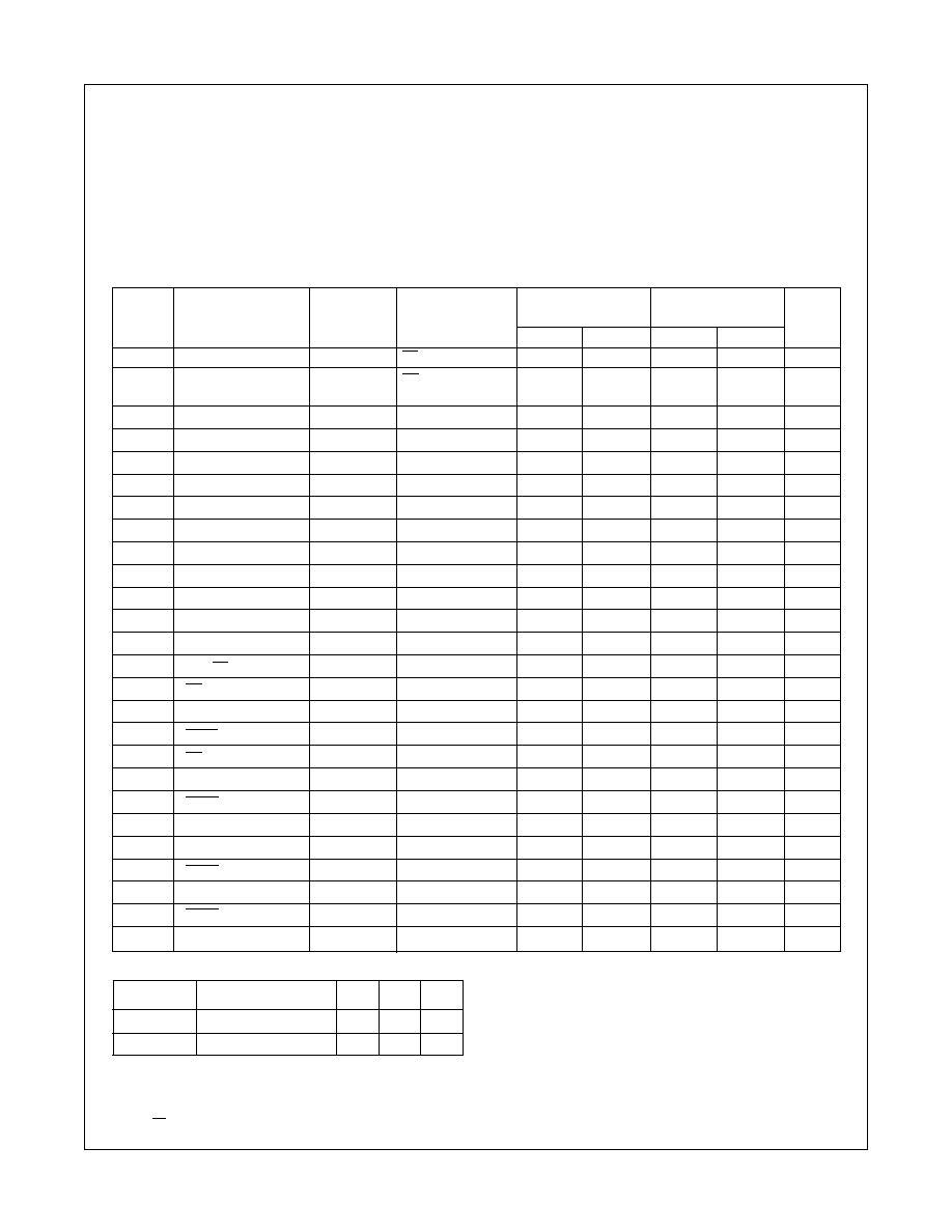
DC and AC Electrical Characteristics
2.7V
V
CC
4.5V (unless otherwise specified)
25C160L/LE
25C160LV
25C160LZ/LZE
Symbol
Parameter
Part
Conditions
Min.
Max.
Min
Max
Units
I
CC
Operating Current
CS = V
IL
3
3
mA
I
CCSB
Standby Current
L
CS = V
CC
10
10
µ
A
LZ
1
N/A
µ
A
I
IL
Input Leakage
V
IN
= 0 to V
CC
-1
1
-1
1
µ
A
I
OL
Output Leakage
V
OUT
= GND to V
CC
-1
1
-1
1
µ
A
V
IL
Input Low Voltage
-0.3
V
CC
* 0.3
-0.3
V
CC
* 0.3
V
V
IH
Input High Voltage
0.7 * V
CC
V
CC
+ 0.3
0.7 * V
CC
V
CC
+ 0.3
V
V
OL
Output Low Voltage
I
OL
= 0.8 mA
0.4
0.4
V
V
OH
Output High Voltage
I
OH
= 0.8 mA
V
CC
- 0.8
V
CC
- 0.8
V
f
OP
SCK Frequency
1.0
1.0
MHz
t
RI
Input Rise Time
2.0
2.0
µ
s
t
FI
Input Fall Time
2.0
2.0
µ
s
t
CLH
Clock High Time
(Note 6)
410
410
ns
t
CLL
Clock Low Time
(Note 6)
410
410
ns
t
CSH
Min. CS High Time
(Note 7)
500
500
ns
t
CSS
CS Setup Time
500
500
ns
t
DIS
Data Setup Time
100
100
ns
t
HDS
HOLD Setup Time
240
240
ns
t
CSN
CS Hold Time
500
500
ns
t
DIN
Data Hold Time
100
100
ns
t
HDN
HOLD Hold Time
240
240
ns
t
PD
Output Delay
C
L
= 200 pF
500
500
ns
t
DH
Output Hold Time
0
0
ns
t
LZ
HOLD Output Low Z
240
240
ns
t
DF
Output Disable Time
C
L
= 200 pF
500
500
ns
t
HZ
HOLD to Output Hi Z
240
240
ns
t
WP
Write Cycle Time
1-16 Bytes
15
15
ms
Capacitance
T
A
= 25
°
C, f = 2.1/1 MHz (Note 8)
Symbol
Test
Typ Max Units
C
OUT
Output Capacitance
3
8
pF
C
IN
Input Capacitance
2
6
pF
AC Test Conditions
Output Load
I
OL
= 10
µ
A, I
OH
= 10
µ
A
Input Pulse Levels
0.3V to 3.5V
Timing Measurement Reference Level
Input
0.4V and 1.6V
Output
0.8V and 1.6V
Note 5: Stress above those listed under "Absolute Maximum Ratings" may cause permanent damage to the device. This is a stress rating only, and functional operation of the device
at these or any other conditions above those indicated in the operational sections of the specification is not implied. Exposure to absolute maximum rating conditions for extended
periods may affect device reliability.
Note 6: The f
OP
frequency specification specifies a minimum clock period of 1/f
OP
. Therefore, for every f
OP
clock cycle, t
CLH
+ t
CLL
must be equal to or greater than 1/f
OP
. For
example, if the 2.1MHz period = 476ns and t
CLH
= 190ns, t
CLL
must be 286ns.
Note 7: CS must be brought high for a minimum of t
CSH
between consecutive instruction cycles.
Note 8: This parameter is periodically sampled and not 100% tested.
5
www.fairchildsemi.com
NM25C160 Rev. D.1
NM25C160 16K-Bit Serial CMOS EEPROM
(Serial Periphrial Interface (SPI) Synchronous Bus)
AC Test Conditions
(Continued)
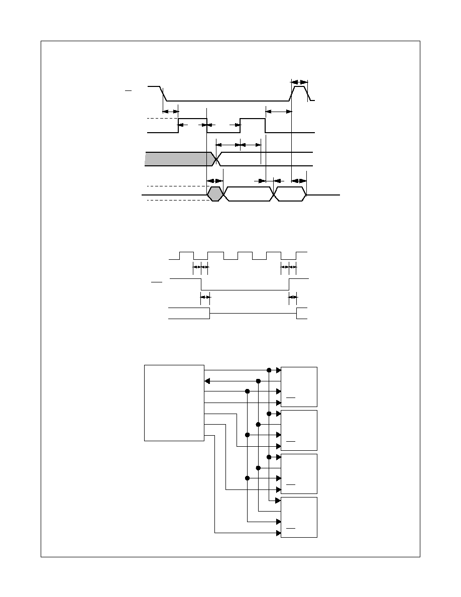
FIGURE 1. Synchronous Data Timing Diagram
FIGURE 3. SPI Serial Interface
SI
SO
SCK
CS
DATA OUT (MOSI)
DATA IN (MISO)
SERIAL CLOCK (CLK)
SS0
SS1
SS2
SS3
SI
SO
SCK
CS
SI
SO
SCK
CS
SI
SO
SCK
CS
SPI
CHIP
SELECTION
MASTER MCU
NM25C16
DS012402-3
DS012402-4
SCK
HOLD
SO
tHZ
tHDN
tHDS
tHDN
tHDS
tLZ
DS012402-6
FIGURE 2. HOLD Timing
,
,,
CS
SCK
SI
SO
VIH
VIL
VIH
VIL
VIH
VIL
VOH
VOL
tCSS
tCSH
tCSN
tDIS
tPD
tDH
tDF
tDIN
tCLH
tCLL