 | ÐлекÑÑоннÑй компоненÑ: NM27C64 | СкаÑаÑÑ:  PDF PDF  ZIP ZIP |
Äîêóìåíòàöèÿ è îïèñàíèÿ www.docs.chipfind.ru
www.fairchildsemi.com
NMC27C64 Rev. C
N
M
C
2
7
C
6
4
6
5
,
5
3
6
-
B
i
t
(
8
1
9
2
x
8
)
C
M
O
S
E
P
R
O
M
NMC27C64
65,536-Bit (8192 x 8) CMOS EPROM
General Description
The NMC27C64 is a 64K UV erasable, electrically reprogrammable
and one-time programmable (OTP) CMOS EPROM ideally suited
for applications where fast turnaround, pattern experimentation
and low power consumption are important requirements.
The NMC27C64 is designed to operate with a single +5V power
supply with 10% tolerance. The CMOS design allows the part to
operate over extended and military temperature ranges.
The NMC27C64Q is packaged in a 28-pin dual-in-line package
with a quartz window. The quartz window allows the user to
expose the chip to ultraviolet light to erase the bit pattern. A new
pattern can then be written electrically into the device by following
the programming procedure.
The NMC27C64N is packaged in a 28-pin dual-in-line plastic
molded package without a transparent lid. This part is ideally
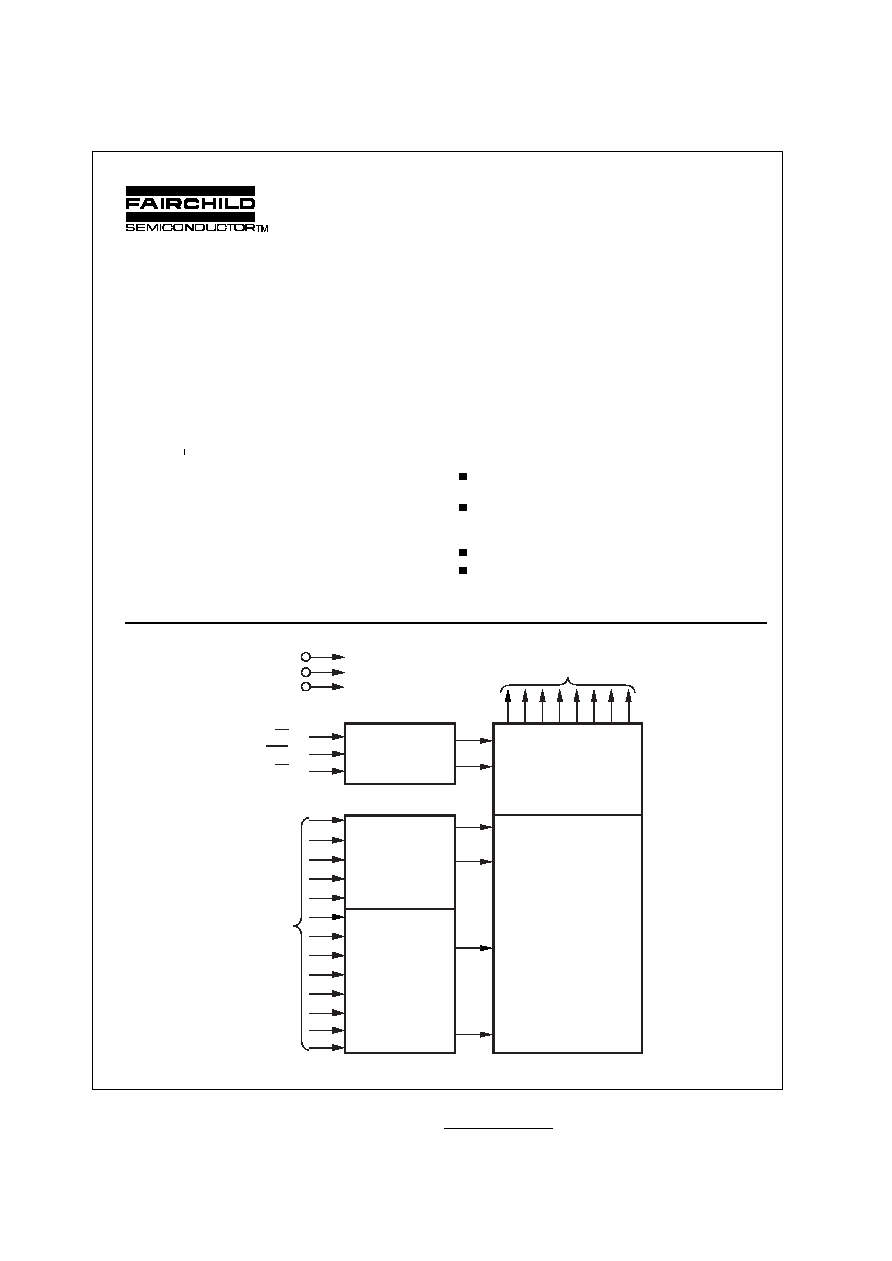
Block Diagram
January 1999
suited for high volume production applications where cost is an
important factor and programming only needs to be done once.
This family of EPROMs are fabricated with Fairchild
'
s proprietary,
time proven CMOS double-poly silicon gate technology which
combines high performance and high density with low power
consumption and excellent reliability.
Features
High performance CMOS
--
150 ns access time
JEDEC standard pin configuration
--
28-pin Plastic DIP package
--
28-pin CERDIP package
Drop-in replacement for 27C64 or 2764
Manufacturers identification code
DS008634-1
Output Enable,
Chip Enable, and
Program Logic
Y Decoder
X Decoder
.
.
.
.
.
.
.
.
.
Output
Buffers
65,536-Bit
Cell Matrix
Data Outputs O0 - O7
VCC
GND
VPP
OE
PGM
CE
A0 - A12
Address
Inputs
©
1998 Fairchild Semiconductor Corporation
2
www.fairchildsemi.com
NMC27C64 Rev. C
N
M
C
2
7
C
6
4
6
5
,
5
3
6
-
B
i
t
(
8
1
9
2
x
8
)
C
M
O
S
E
P
R
O
M
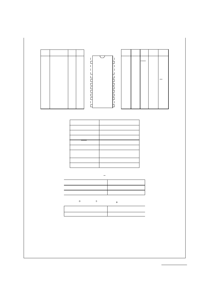
Connection Diagram
Note:
Socket compatible EPROM pin configurations are shown in the blocks adjacent to the NMC27C64 pins.
V
CC
PGM
NC
A8
A9
A11
OE
A10
CE
O7
O6
O5
O4
O3
1
2
3
4
5
6
7
8
9
10
11
12
13
14
28
27
26
25
24
23
22
21
20
19
18
17
16
15
V
PP
A12
A7
A6
A5
A4
A3
A2
A1
A0
O0
O1
O2
GND
A15
A12
A7
A6
A5
A4
A3
A2
A1
A0
O0
O1
O2
GND
27C512
27512
27C256
27256
V
PP
A12
A7
A6
A5
A4
A3
A2
A1
A0
O0
O1
O2
GND
NMC27C64
A7
A6
A5
A4
A3
A2
A1
A0
O0
O1
O2
GND
27C32
2732
A7
A6
A5
A4
A3
A2
A1
A0
O0
O1
O2
GND
27C16
2716
V
PP
A12
A7
A6
A5
A4
A3
A2
A1
A0
O0
O1
O2
GND
27C128
27128
27C256
27256
27C512
27512
V
CC
A14
A13
A8
A9
A11
OE
A10
CE/PGM
O7
O6
O5
O4
O3
V
CC
A14
A13
A8
A9
A11
OE/V
PP
A10
CE
O7
O6
O5
O4
O3
V
CC
PGM
A13
A8
A9
A11
OE
A10
CE
O7
O6
O5
O4
O3
V
CC
A8
A9
V
PP
OE
A10
CE/PGM
O7
O6
O5
O4
O3
V
CC
A8
A9
A11
OE/V
PP
A10
CE
O7
O6
O5
O4
O3
27C16
2716
27C32
2732
27C128
27128
DS008634-2
Pin Names
A0
A12
Addresses
CE
Chip Enable
OE
Output Enable
O
0
O
7
Outputs
PGM
Program
NC
No Connect
V
PP
Programming
Voltage
V
CC
Power Supply
GND
Ground
Commercial Temperature Range
V
CC
= 5V 10%
Parameter/Order Number
Access Time (ns)
NMC27C64Q, N 150
150
NMC27C64Q, N 200
200
Extended Temp Range (-40 C to +85 C)
V
CC
= 5V 10%
Parameter/Order Number
Access Time (ns)
NMC27C64QE, NE200
200
3
www.fairchildsemi.com
NMC27C64 Rev. C
N
M
C
2
7
C
6
4
6
5
,
5
3
6
-
B
i
t
(
8
1
9
2
x
8
)
C
M
O
S
E
P
R
O
M
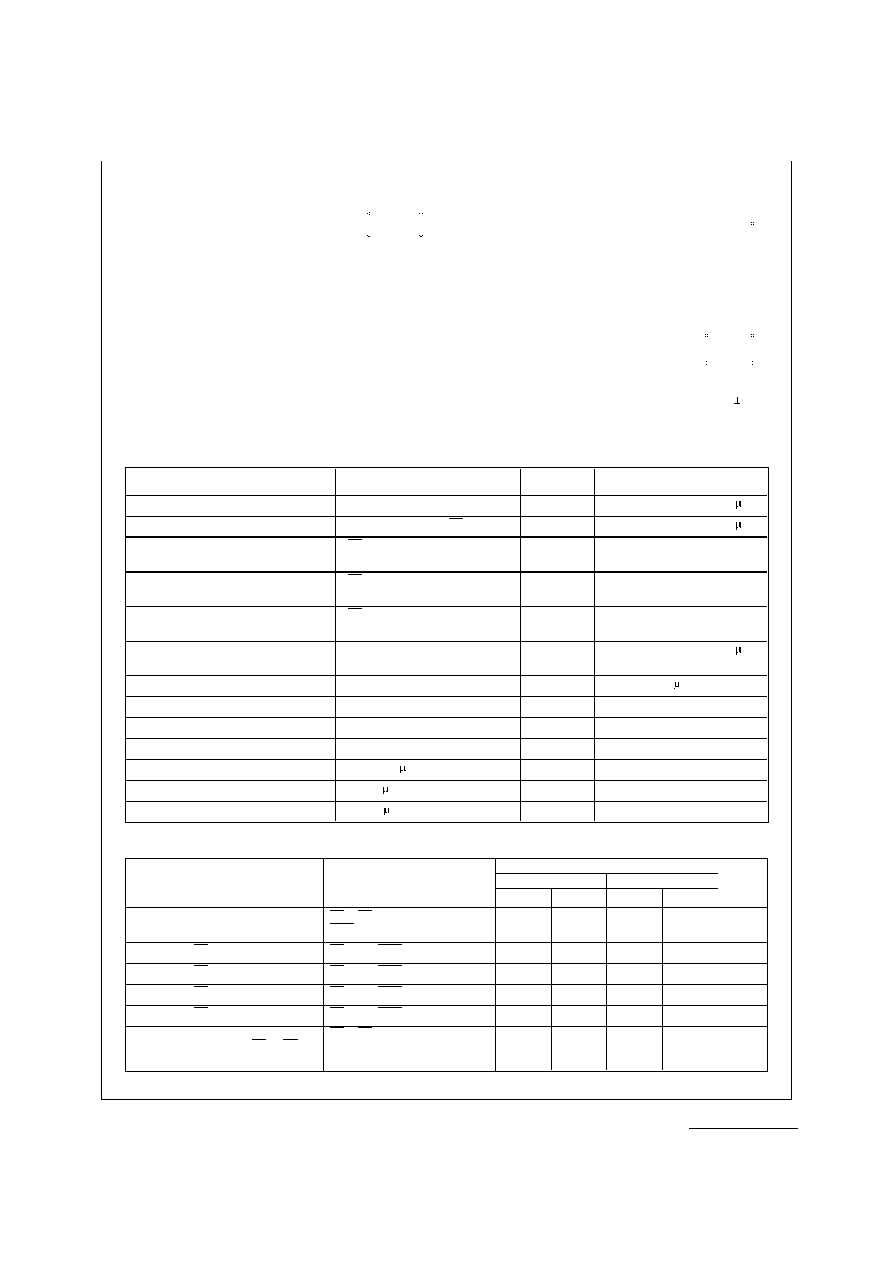
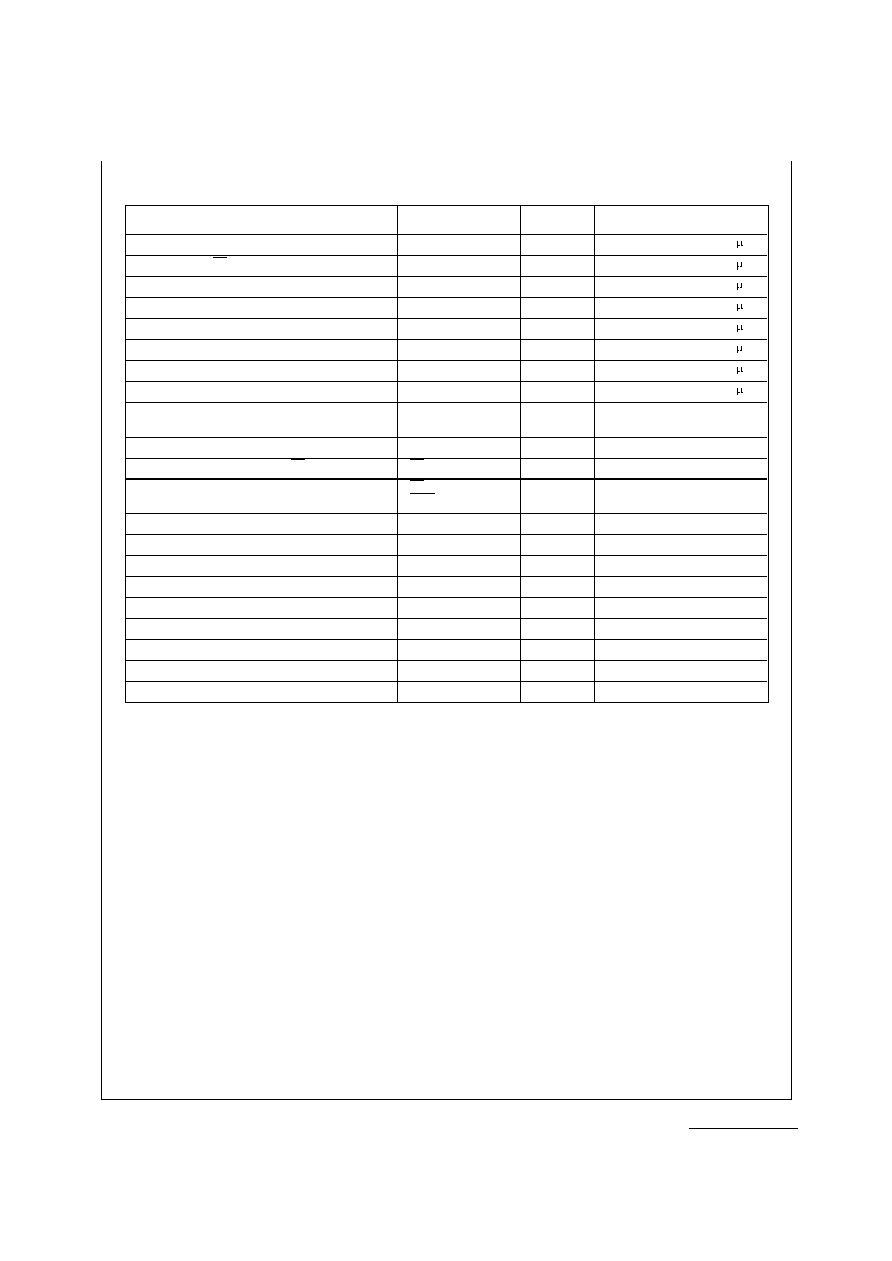
READ OPERATION
DC Electrical Characteristics
Symbol
Parameter
Conditions
Min
Typ
Max
Units
I
LI
Input Load Current
V
IN
= V
CC
or GND
10
A
I
LO
Output Leakage Current
V
OUT
= V
CC
or GND, CE = V
IH
10
A
I
CC1
V
CC
Current (Active)
CE = V
IL
,f=5 MHz
5
20
mA
(Note 9)
TTL Inputs
Inputs = V
IH
or V
IL
, I/O = 0 mA
I
CC2
V
CC
Current (Active)
CE = GND, f = 5 MHz
3
10
mA
(Note 9)
CMOS Inputs
Inputs = V
CC
or GND, I/O = 0 mA
I
CCSB1
V
CC
Current (Standby)
CE = V
IH
0.1
1
mA
TTL Inputs
I
CCSB2
V
CC
Current (Standby)
CE = V
CC
0.5
100
A
CMOS Inputs
I
PP
VPP Load Current
V
PP
= V
CC
10
A
V
IL
Input Low Voltage
-0.1
0.8
V
V
IH
Input High Voltage
2.0
V
CC
+1
V
V
OL1
Output Low Voltage
I
OL
= 2.1 mA
0.45
V
V
OH1
Output High Voltage
I
OH
= -400 A
2.4
V
V
OL2
Output Low Voltage
I
OL
= 0 A
0.1
V
V
OH2
Output High Voltage
I
OH
= 0 A
V
CC
- 0.1
V
AC Electrical Characteristics
NMC27C64
Symbol
Parameter
Conditions
150
200, E200
Units
Min
Max
Min
Max
t
ACC
Address to
CE = OE = V
IL
150
200
ns
Output Delay
PGM = V
IH
t
CE
CE to Output Delay
OE = V
IL
, PGM = V
IH
150
200
ns
t
OE
OE to Output Delay
CE = V
IL
, PGM = V
IH
60
60
ns
t
DF
OE High to Output Float
CE = V
IL
, PGM = V
IH
0
60
0
60
ns
t
CF
CE High to Output Float
OE = V
IL
, PGM = V
IH
0
60
0
60
ns
t
OH
Output Hold from
CE = OE = V
IL
Addresses, CE or OE ,
PGM = V
IH
0
0
ns
Whichever Occurred First
Absolute Maximum Ratings
(Note 1)
Temperature Under Bias
-55 C to +125 C
Storage Temperature
-65 C to +150 C
All Input Voltages except A9
with Respect to Ground (Note 10)
+6.5V to -0.6V
All Output Voltages
with Respect to Ground (Note 10)V
CC
+1.0V to GND -0.6V
V
PP
Supply Voltage and A
9
with Respect to Ground
During Programming
+14.0V to -0.6V
V
CC
Supply Voltage with
Respect to Ground
+7.0V to -0.6V
Power Dissipation
1.0W
Lead Temperature
(Soldering, 10 sec.)
300 C
ESD Rating
(Mil Spec 883C,
Method 3015.2)
2000V
Operating Conditions
(Note 7)
Temperature Range
NMC27C64Q 150, 200
0 C to +70 C
NMC27C64N 150, 200
NMC27C64QE 200
-40 C to +85 C
NMC27C64NE 200
V
CC
Power Supply
+5V 10%
4
www.fairchildsemi.com
NMC27C64 Rev. C
N
M
C
2
7
C
6
4
6
5
,
5
3
6
-
B
i
t
(
8
1
9
2
x
8
)
C
M
O
S
E
P
R
O
M
Capacitance
TA = +25
°
C, f = 1 MHz (Note 2) NMC27C64Q
Symbol
Parameter
Conditions
Typ
Max
Units
C
IN
Input Capacitance
V
IN
= 0V
6
8
pF
C
OUT
Output Capacitance
V
OUT
= 0V
9
12
pF
Capacitance
TA = +25
°
C, f = 1 MHz (Note 2) NMC27C64N
Symbol
Parameter
Conditions
Typ
Max
Units
C
IN
Input Capacitance
V
IN
= 0V
5
10
pF
C
OUT
Output Capacitance
V
OUT
= 0V
8
10
pF
AC Test Conditions
Output Load
1 TTL Gate and C
L
= 100 pF (Note 8)
Input Rise and Fall Times
5 ns
Input Pulse Levels
0.45V to 2.4V
Timing Measurement Reference Level
Inputs
0.8V and 2V
Outputs
0.8V and 2V
AC Waveforms
(Note 6) (Note 9)
Note 1: Stresses above those listed under
"
Absolute Maximum Ratings
"
may cause permanent damage to the device. This is a stress rating only and functional operation of
the device at these or any other conditions above those indicated in the operational sections of this specification is not implied. Exposure to absolute maximum rating conditions
for extended periods may affect device reliability.
Note 2: This parameter is only sampled and is not 100% tested.
Note 3: OE may be delayed up to t
ACC
- t
OE
after the falling edge of CE without impacting t
ACC
.
Note 4: The t
DF
and t
CF
compare level is determined as follows:
High to TRI-STATE
®
, the measured V
OH1
(DC)
0.10V;
Low to TRI-STATE, the measured V
OL1
(DC) + 0.10V.
Note 5: TRI-STATE may be attained using OE or CE .
Note 6: The power switching characteristics of EPROMs require careful device decoupling. It is recommended that at least a 0.1 F ceramic capacitor be used on every device
between V
CC
and GND.
Note 7: The outputs must be restricted to V
CC
+ 1.0V to avoid latch-up and device damage.
Note 8: 1 TTL Gate: I
OL
= 1.6 mA, I
OH
= -400 A.
C
L
: 100 pF includes fixture capacitance.
Note 9: V
PP
may be connected to V
CC
except during programming.
Note 10: Inputs and outputs can undershoot to -2.0V for 20 ns Max.
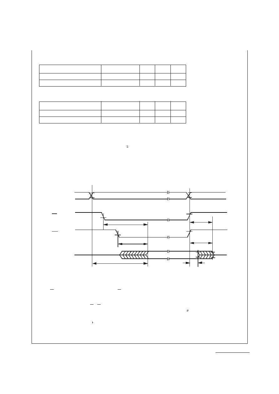
Address Valid
Valid Output
Hi-Z
2V
0.8V
2V
0.8V
2V
0.8V
ADDRESS
OUTPUT
CE
OE
t
CE
2V
0.8V
(Note 3)
(Note 3)
t
DF
t
CF
(Notes 4, 5)
(Notes 4, 5)
t
OH
Hi-Z
t
OE
ACC
t
5
www.fairchildsemi.com
NMC27C64 Rev. C
N
M
C
2
7
C
6
4
6
5
,
5
3
6
-
B
i
t
(
8
1
9
2
x
8
)
C
M
O
S
E
P
R
O
M
Programming Characteristics
(Note 11) (Note 12) (Note 13) (Note 14)
Symbol
Parameter
Conditions
Min
Typ
Max
Units
t
AS
Address Setup Time
2
s
t
OES
OE Setup Time
2
s
t
CES
CE Setup Time
2
s
t
DS
Data Setup Time
2
s
t
VPS
V
PP
Setup Time
2
s
t
VCS
V
CC
Setup Time
2
s
t
AH
Address Hold Time
0
s
t
DH
Data Hold Time
2
s
t
DF
Output Enable to
CE = V
IL
0
130
ns
Output Float Delay
t
PW
Program Pulse Width
0.45
0.5
0.55
ms
t
OE
Data Valid from OE
CE = V
IL
150
ns
I
PP
V
PP
Supply Current During
CE = V
IL
30
mA
Programming Pulse
PGM = V
IL
I
CC
V
CC
Supply Current
10
mA
T
A
Temperature Ambient
20
25
30
°
C
V
CC
Power Supply Voltage
5.75
6.0
6.25
V
V
PP
Programming Supply Voltage
12.2
13.0
13.3
V
t
FR
Input Rise, Fall Time
5
ns
V
IL
Input Low Voltage
0.0
0.45
V
V
IH
Input High Voltage
2.4
4.0
V
t
IN
Input Timing Reference Voltage
0.8
1.5
2.0
V
t
OUT
Output Timing Reference Voltage
0.8
1.5
2.0
V