 | ÐлекÑÑоннÑй компоненÑ: NM34W02 | СкаÑаÑÑ:  PDF PDF  ZIP ZIP |
Äîêóìåíòàöèÿ è îïèñàíèÿ www.docs.chipfind.ru
1
www.fairchildsemi.com
NM34W02 Rev. C.2
NM34W02 2K-Bit Standard 2-Wire Bus Interface Serial EEPROM
with Full Array Write Protect
© 1999 Fairchild Semiconductor Corporation
NM34W02
2K-Bit Standard 2-Wire Bus Interface Serial EEPROM
with Full Array Write Protect
Designed with Permanent Write-Protection for First 128 Bytes for Serial Presence
Detect Application on Memory Modules (PC100 Compliant)
General Description
The NM34W02 is 2048 bits of CMOS non-volatile electrically
erasable memory. This device is specifically designed to support
Serial Presence Detect circuitry in memory modules. This com-
munications protocol uses CLOCK (SCL) and DATA I/O (SDA)
lines to synchronously clock data between the master (for ex-
ample a microprocessor) and the slave EEPROM device(s).
The contents of the non-volatile memory allows the CPU to
determine the capacity of the module and the electrical character-
istics of the memory devices it contains. This will enable "plug and
play" capability as the module is read and PC main memory
resources utilized through the memory controller.
The first 128 bytes of the memory of the NM34W02 can be
permanently Write Protected by writing to the "WRITE PROTECT"
Register. Write Protect implementation details are described
under the section titled Addressing the WP Register. In addition,
like the NM24Wxx product family, the entire memory array can be
write-protected through "WP" pin.
The NM34W02 is available in a JEDEC standard TSSOP package
for low profile memory modules for systems requiring efficient
space utilization such as in a notebook computer. Two options are
available: L - Low Voltage and LZ - Low Power, allowing the part
to be used in systems where battery life is of primary importance.
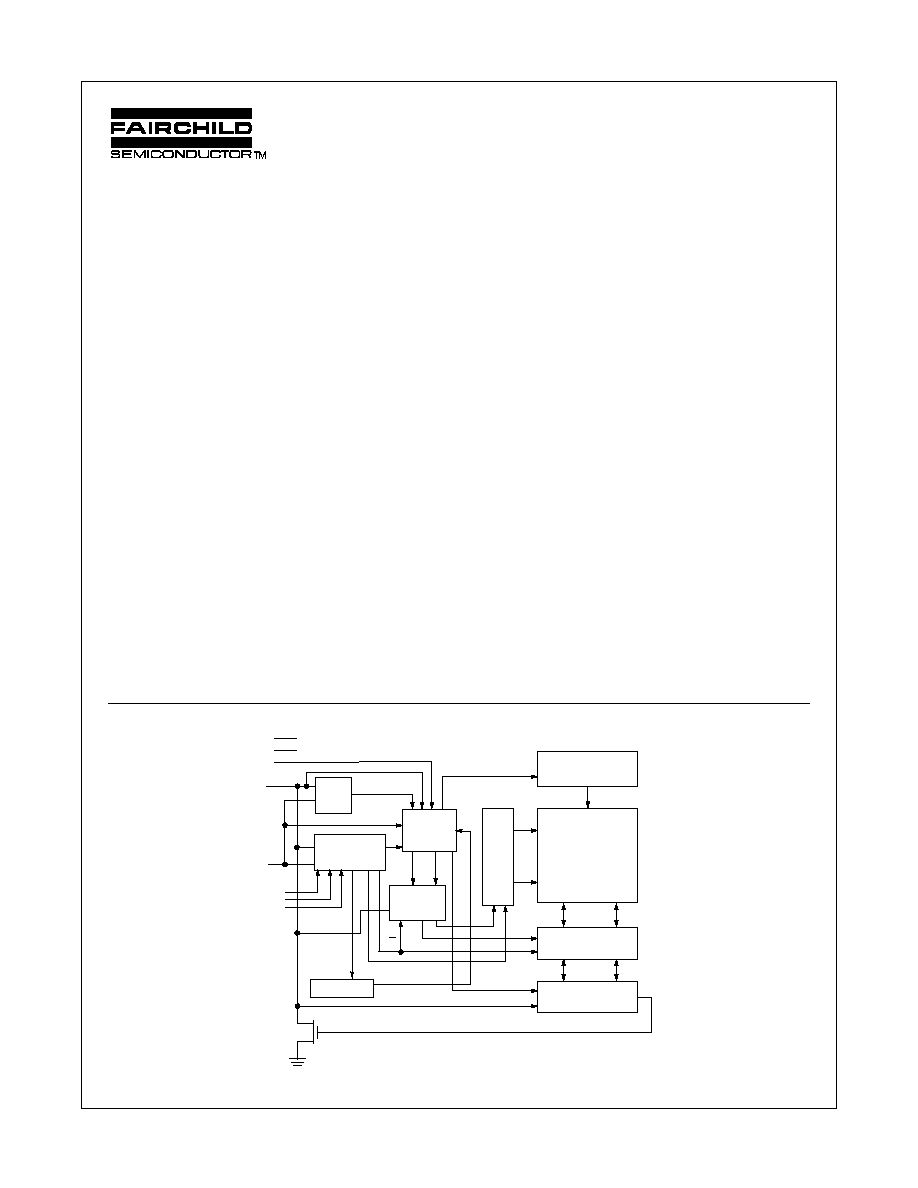
Block Diagram
Features
s
PC100 Compliant
s
Extended Operating Voltage: 2.7V-5.5V
s
Software Write-Protection for first 128 bytes
s
Hardware Write-Protection for entire memory array
s
200
µ
A active current typical
1.0
µ
A standby current typical (L)
0.1
µ
A standby current typical (LZ)
s
IIC compatible interface
Provides bidirectional data transfer protocol
s
Sixteen byte page write mode
Minimizes total write time per byte
s
Self timed write cycle
- Typical write cycle time of 6ms
s
Endurance: 1,000,000 data changes
s
Data retention greater than 40 years
s
Packages available: 8-pin TSSOP and 8-pin SO
s
Temperature Ranges: Commercial and Extended
DS500078-1
H.V. GENERATION
TIMING &CONTROL
E2PROM
ARRAY
16 x 16 x 8
16
YDEC
8
DATA REGISTER
XDEC
CONTROL
LOGIC
WORD
ADDRESS
COUNTER
SLAVE ADDRESS
REGISTER &
COMPARATOR
START
STOP
LOGIC
START CYCLE
16
4
4
CK
DIN
R/W
LOAD
INC
SDA
VSS
VCC
WP
DOUT
A2
A1
A0
Device Address Bits
0/1/2/3
SCL
Write Protect
Register
March 1999
2
www.fairchildsemi.com
NM34W02 Rev. C.2
NM34W02 2K-Bit Standard 2-Wire Bus Interface Serial EEPROM
with Full Array Write Protect
A0
A1
A2
VSS
VCC
WP
SCL
SDA
8
7
6
5
1
2
3
4
NM34W02
DS500078-2
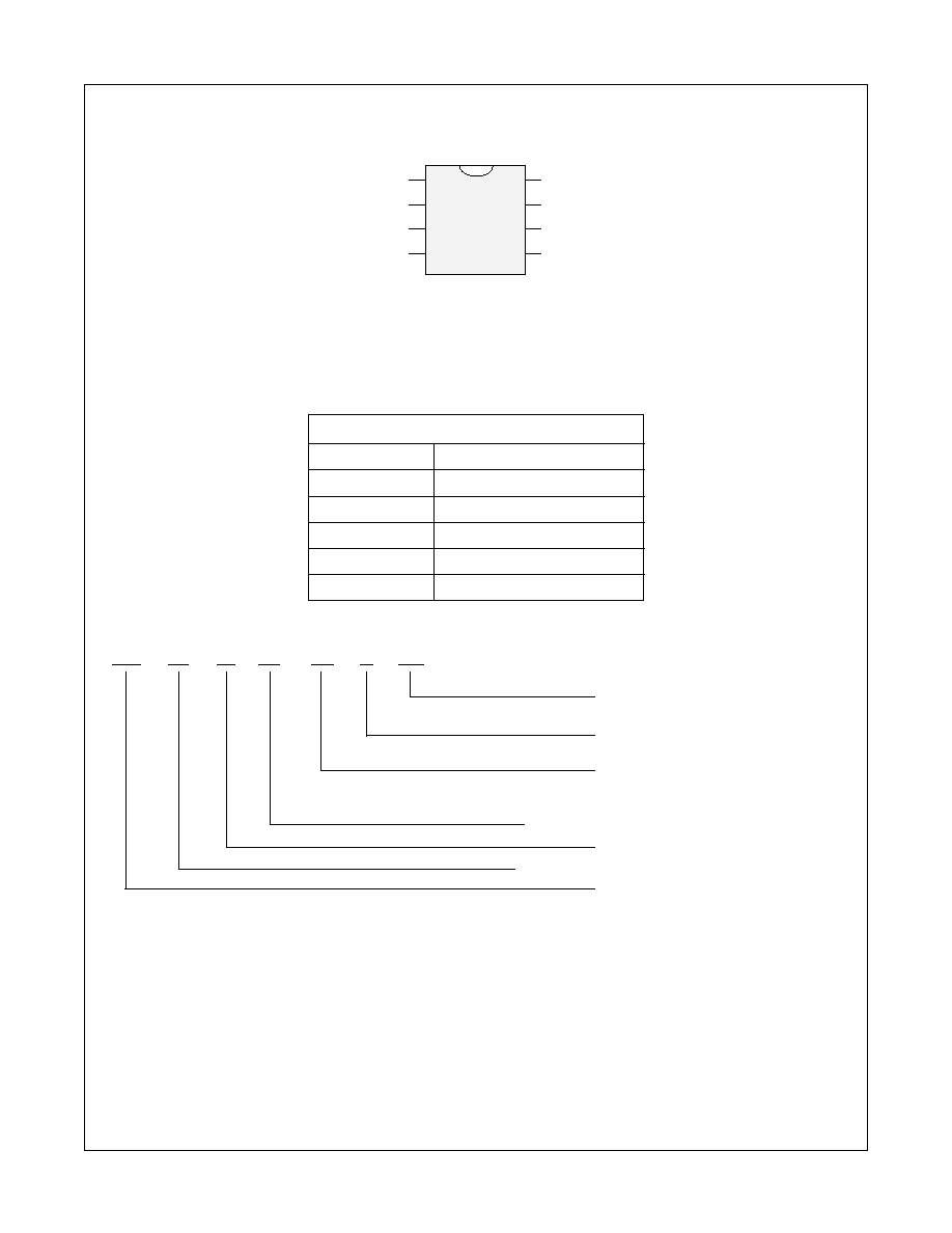
SO (M8) and TSSOP (MT8) Package
Connection Diagram
Top View
See Package Number
M08A and MTC08
Pin Names
A0,A1,A2
Device Address Inputs
V
SS
Ground
SDA
Data I/O
SCL
Clock Input
WP
Write Protect
V
CC
Power Supply
Ordering Information
NM
34
W
02
LZ
E
XX
Letter
Description
Package
M8
8-Pin SO8
MT8
8-Pin TSSOP
Temp. Range
None
0 to 70
°
C
E
-40 to +85
°
C
Voltage Operating Range
Blank
4.5V to 5.5V
L
2.7V to 4.5V
LZ
2.7V to 4.5V and
<1
µ
A Standby Current
Density
02
2K
W
Full Array Write Protect
Interface
34
IIC
NM
Fairchild Non-Volatile
Memory
3
www.fairchildsemi.com
NM34W02 Rev. C.2
NM34W02 2K-Bit Standard 2-Wire Bus Interface Serial EEPROM
with Full Array Write Protect
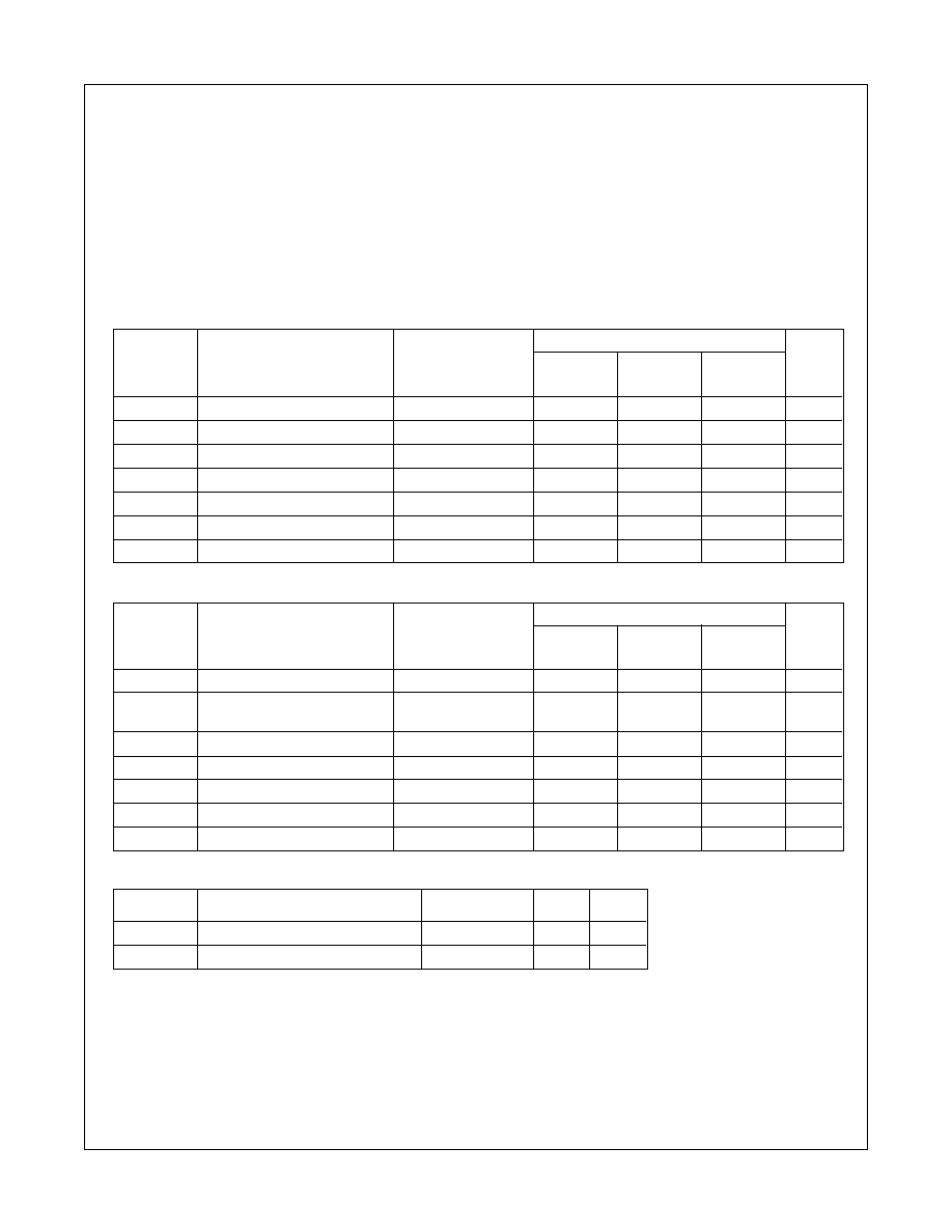
Product Specifications
Absolute Maximum Ratings
Ambient Storage Temperature
65
°
C to +150
°
C
All Input or Output Voltages
with Respect to Ground
6.5V to 0.3V
Lead Temperature
(Soldering, 10 seconds)
+300
°
C
ESD Rating
2000V min.
Operating Conditions
Ambient Operating Temperature
NM34W02
0
°
C to +70
°
C
NM34W02E
-40
°
C to +85
°
C
Positive Power Supply
NM34W02
4.5V to 5.5V
NM34W02L
2.7V to 4.5V
NM34W02LZ
2.7V to 4.5V
Standard V
CC
(4.5V to 5.5V) DC Electrical Characteristics
Symbol
Parameter
Test Conditions
Limits
Units
Min
Typ
Max
(Note 1)
I
CCA
Active Power Supply Current
f
SCL
= 100 kHz
0.2
1.0
mA
I
SB
Standby Current
V
IN
= GND or V
CC
10
50
µ
A
I
LI
Input Leakage Current
V
IN
= GND to V
CC
0.1
1
µ
A
I
LO
Output Leakage Current
V
OUT
= GND to V
CC
0.1
1
µ
A
V
IL
Input Low Voltage
0.3
V
CC
x 0.3
V
V
IH
Input High Voltage
V
CC
x 0.7
V
CC
+ 0.5
V
V
OL
Output Low Voltage
I
OL
= 3 mA
0.4
V
Low V
CC
(2.7V to 5.5V) DC Electrical Characteristics
Symbol
Parameter
Test Conditions
Limits
Units
Min
Typ
Max
(Note 1)
I
CCA
Active Power Supply Current
f
SCL
= 100 kHz
0.2
1.0
mA
I
SB
Standby Current for L
V
IN
= GND or V
CC
1
10
µ
A
Standby Current for LZ
V
IN
= GND or V
CC
0.1
1
µ
A
I
LI
Input Leakage Current
V
IN
= GND to V
CC
0.1
1
µ
A
I
LO
Output Leakage Current
V
OUT
= GND to V
CC
0.1
1
µ
A
V
IL
Input Low Voltage
0.3
V
CC
x 0.3
V
V
IH
Input High Voltage
V
CC
x 0.7
V
CC
+ 0.5
V
V
OL
Output Low Voltage
I
OL
= 3 mA
0.4
V
Capacitance
T
A
= +25
°
C, f = 100/400 KHz, V
CC
= 5V
(Note 2)
Symbol
Test
Conditions
Max
Units
C
I/O
Input/Output Capacitance (SDA)
V
I/O
= 0V
8
pF
C
IN
Input Capacitance (A0, A1, A2, SCL)
V
IN
= 0V
6
pF
Note 1: Typical values are T
A
= 25
°
C and nominal supply voltage (5V).
Note 2: This parameter is periodically sampled and not 100% tested.
4
www.fairchildsemi.com
NM34W02 Rev. C.2
NM34W02 2K-Bit Standard 2-Wire Bus Interface Serial EEPROM
with Full Array Write Protect
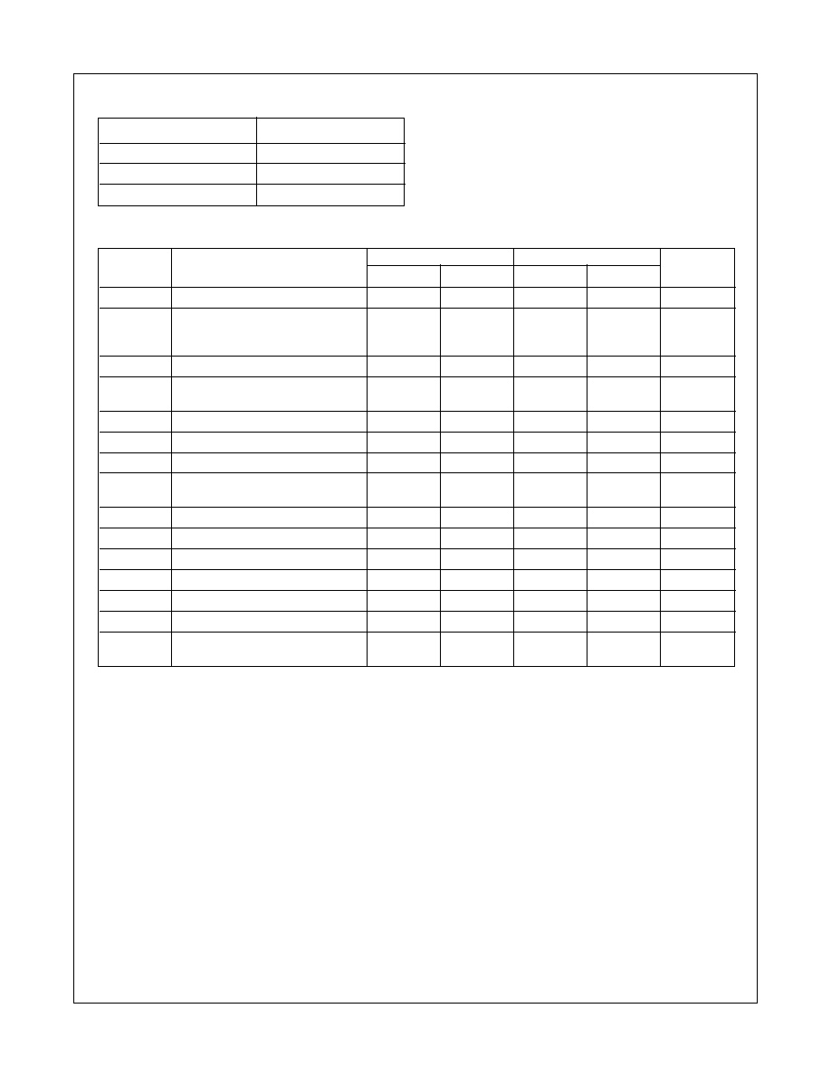
AC Conditions of Test
Input Pulse Levels
V
CC
x 0.1 to V
CC
x 0.9
Input Rise and Fall Times
10 ns
Input & Output Timing Levels
V
CC
x 0.5
Output Load
1 TTL Gate and C
L
= 100 pF
Read and Write Cycle Limits (Standard and Low V
CC
Range 2.7V - 5.5V)
Symbol
Parameter
100 KHz
400 KHz
Units
Min
Max
Min
Max
f
SCL
SCL Clock Frequency
100
400
KHz
T
I
Noise Suppression Time Constant at
SCL, SDA Inputs (Minimum V
IN
100
50
ns
Pulse width)
t
AA
SCL Low to SDA Data Out Valid
0.3
3.5
0.1
0.9
µ
s
t
BUF
Time the Bus Must Be Free before
4.7
1.3
µ
s
a New Transmission Can Start
t
HD:STA
Start Condition Hold Time
4.0
0.6
µ
s
t
LOW
Clock Low Period
4.7
1.5
µ
s
t
HIGH
Clock High Period
4.0
0.6
µ
s
t
SU:STA
Start Condition Setup Time
4.7
0.6
µ
s
(for a Repeated Start Condition)
t
HD:DAT
Data in Hold Time
0
0
ns
t
SU:DAT
Data in Setup Time
250
100
ns
t
R
SDA and SCL Rise Time
1
0.3
µ
s
t
F
SDA and SCL Fall Time
300
300
ns
t
SU:STO
Stop Condition Setup Time
4.7
0.6
µ
s
t
DH
Data Out Hold Time
300
50
ns
t
WR
Write Cycle Time - NM34W02
10
10
ms
(Note 3)
- NM34W02L, NM34W02LZ
15
15
Note 3: The write cycle time (t
WR
) is the time from a valid stop condition of a write sequence to the end of the internal erase/program cycle. During the write cycle, the
NM34W02 bus interface circuits are disabled, SDA is allowed to remain high per the bus-level pull-up resistor, and the device does not respond to its slave address.
5
www.fairchildsemi.com
NM34W02 Rev. C.2
NM34W02 2K-Bit Standard 2-Wire Bus Interface Serial EEPROM
with Full Array Write Protect
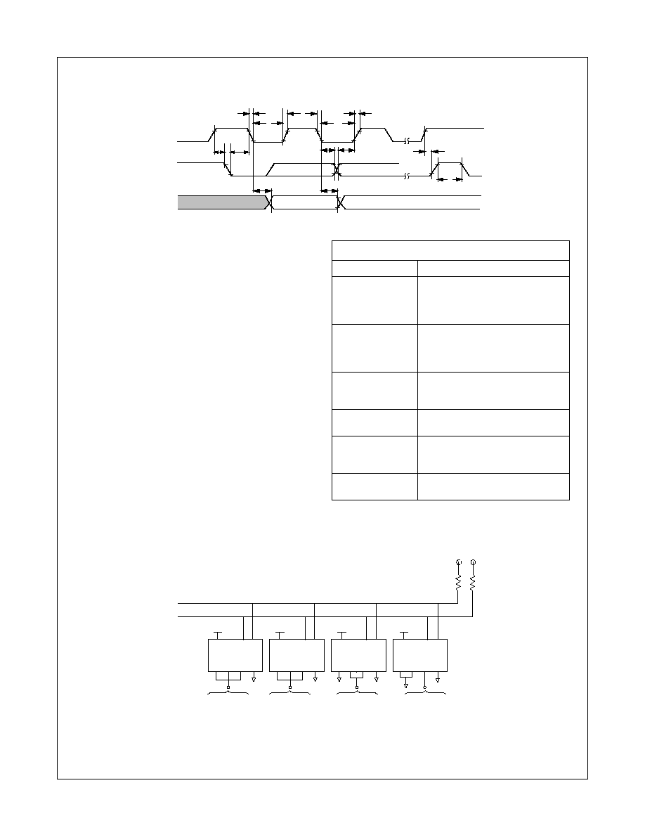
Bus Timing
Background Information (IIC Bus)
As mentioned, the IIC bus allows synchronous bidirectional com-
munication between Transmitter/Receiver using the SCL (clock)
and SDA (Data I/O) lines. All communication must be started with
a valid START condition, concluded with a STOP condition and
acknowledged by the Receiver with an ACKNOWLEDGE condi-
tion.
In addition, since the IIC bus is designed to support other devices
such as RAM, EPROMs, etc., a device type identifier string must
follow the START condition. For EEPROMs, this 4-bit string is
1010. Also refer the Addressing the WP Register section.
As shown below, although the EEPROMs on the IIC bus may be
configured in any manner required, the total memory addressed
can not exceed 16K (16,384 bits) on the Standard IIC. EEPROM
memory address programming is controlled by 2 methods:
· Hardware configuring the A0, A1, and A2 pins (Device
Address pins) with pull-up or pull-down to V
CC
or V
SS
. All
unused pins must be grounded (tied to V
SS
).
· Software addressing the required PAGE BLOCK within the
device memory array (as sent in the Slave Address string).
Addressing an EEPROM memory location involves sending a
command string with the following information:
[DEVICE TYPE]--[DEVICE ADDRESS]--[PAGE BLOCK
ADDRESS]--[BYTE ADDRESS]
DEFINITIONS
BYTE
8 bits of data
PAGE
16 sequential addresses (one byte
each) that may be programmed
during a 'Page Write' programming
cycle
PAGE BLOCK
2,048 (2K) bits organized into 16
pages of addressable memory. (8
bits) x (16 bytes) x (16 pages) = 2,048
bits
MASTER
Any IIC device CONTROLLING the
transfer of data (such as a micropro-
cessor)
SLAVE
Device being controlled (EEPROMs
are always considered Slaves)
TRANSMITTER
Device currently SENDING data on
the bus (may be either a Master or
Slave).
RECEIVER
Device currently receiving data on the
bus (Master or Slave)
Example of 16K of Memory on 2-Wire Bus
Note:
The SDA pull-up resistor is required due to the open-drain/open collector output of IIC bus devices.
The SCL pull-up resistor is recommended because of the normal SCL line inactive 'high' state.
It is recommended that the total line capacitance be less than 400pF.
Specific timing and addressing considerations are described in greater detail in the following sections.
,,
SCL
SDA
IN
SDA
OUT
tF
tLOW
tHIGH
tR
tLOW
tAA
tDH
tBUF
tSU:STA
tHD:DAT
tHD:STA
tSU:DAT
tSU:STO
DS500078-5
DS500078-6
SDA
SCL
NM34C02L
VCC
VCC
A0 A1 A2 VSS
NM24C02
A0 A1 A2 VSS
NM24C04
A0 A1 A2 VSS
NM24C08
A0 A1 A2 VSS
VCC
To V
CC
or V
SS
To V
CC
or V
SS
To V
CC
or V
SS
To V
CC
or V
SS
VCC
VCC
VCC