 | ÐлекÑÑоннÑй компоненÑ: QRB1114 | СкаÑаÑÑ:  PDF PDF  ZIP ZIP |
Äîêóìåíòàöèÿ è îïèñàíèÿ www.docs.chipfind.ru
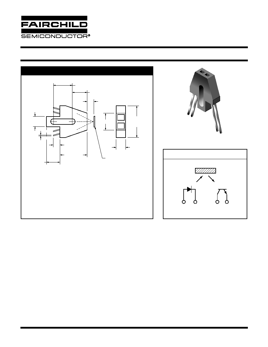
PACKAGE DIMENSIONS
SCHEMATIC
PHOTOTRANSISTOR
REFLECTIVE OBJECT SENSOR
QRB1113 QRB1114
3/5/02 DS300350
Page 1 of 4
© 2002 Fairchild Semiconductor Corporation
E
S
DESCRIPTION
The QRB1113/1114 consists of an infrared emitting diode and an NPN silicon phototransistor mounted side by side on a converg-
ing optical axis in a black plastic housing. The phototransistor responds to radiation from the emitting diode only when a reflective
object passes within its field of view. The area of the optimum response approximates a circle .200" in diameter.
FEATURES
·
No contact surface sensing
·
Phototransistor output
·
Focused for sensing specular reflection
·
Daylight filter on photosensor
·
Dust cover
0.210 (5.33)
0.420 (10.67)
0.328 (8.33)
0.373 (9.47)
0.703 (17.86)
0.150 (3.81)
MIN
0.603 (15.32)
0.300 (7.62)
0.226 (5.74)
0.150 (3.81)
NOM
0.020 (0.51)
4X
PIN1 ANODE
PIN2 CATHODE
PIN3 EMITTER
PIN4 COLLECTOR
PIN 1
PIN 2
PIN 3
PIN 4
REFLECTIVE
SURFACE
ES
1
2
3
4
NOTES:
1. Dimensions for all drawings are in inches (mm).
2. Tolerance of ± .010 (.25) on all non-nominal dimensions unless
otherwise specified.

PHOTOTRANSISTOR
REFLECTIVE OBJECT SENSOR
QRB1113 QRB1114
3/5/02 DS300350
Page 2 of 4
© 2002 Fairchild Semiconductor Corporation
NOTES
1. Derate power dissipation linearly 1.67 mW/°C above 25°C.
2. RMA flux is recommended.
3. Methanol or isopropyl alcohols are recommended as cleaning agents.
4. Soldering iron 1/16" (1.6mm) minimum from housing.
5. D is the distance from the assembly face to the reflective surface.
6. Measured using an Eastman Kodak neutral test card with 90% diffused reflecting surface.
7. Cross talk is the photo current measured with current to the input diode and no reflecting surface.
ABSOLUTE MAXIMUM RATINGS
(T
A
= 25°C unless otherwise specified)
Parameter
Symbol
Rating
Units
Operating Temperature
T
OPR
-40 to +85
°C
Storage Temperature
T
STG
-40 to +85
°C
Soldering Temperature (Iron)
(2,3,4)
T
SOL-I
240 for 5 sec
°C
Soldering Temperature (Flow)
(2,3)
T
SOL-F
260 for 10 sec
°C
EMITTER
Continuous Forward Current
I
F
50
mA
Reverse Voltage
V
R
5
V
Power Dissipation
(1)
P
D
100
mW
SENSOR
Collector-Emitter Voltage
V
CEO
30
V
Emitter-Collector Voltage
V
ECO
4.5
V
Collector Current
20
mA
Power Dissipation
(1)
P
D
100
mW
ELECTRICAL/OPTICAL CHARACTERISTICS
(T
A
= 25°C)
Parameter
Test Conditions
Symbol
Min.
Typ.
Max.
Units
EMITTER
Forward Voltage
I
F
= 40 mA
V
F
--
--
1.7
V
Reverse Current
V
R
= 5.0 V
I
R
--
--
100
µA
Peak Emission Wavelength
I
F
= 20 mA
PE
--
940
--
nm
SENSOR
Collector-Emitter Breakdown Voltage
I
C
= 1 mA
BV
CEO
30
--
--
V
Emitter-Collector Breakdown Voltage
I
E
= 0.1 mA
BV
ECO
5
--
--
V
Collector-Emitter Dark Current
V
CE
= 10 V, I
F
= 0 mA
I
CEO
--
--
100
nA
COUPLED
On-state Collector Current
I
F
= 40 mA, V
CE
= 5 V
D = .150"
(5,6)
I
C(ON)
mA
QRB1113
0.20
--
--
QRB1114
0.60
--
Collector-Emitter
I
F
= 20 mA, I
C
= 0.5 mA
V
CE (SAT)
--
--
0.4
V
Saturation Voltage
Rise Time
V
CE
= 5 V, R
L
= 100 V
I
C(ON)
= 5 mA
t
r
--
8
--
µs
Fall Time
t
f
--
8
--
Cross Talk
I
F
= 40 mA, V
CE
= 5 V
(7)
I
CX
--
--
1.00
µA
PHOTOTRANSISTOR
REFLECTIVE OBJECT SENSOR
QRB1113 QRB1114
3/5/02 DS300350
Page 3 of 4
© 2002 Fairchild Semiconductor Corporation
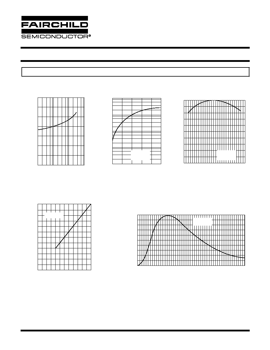
TYPICAL PERFORMANCE CURVES
1.60
10.0
1.00
1.00
0.8
0.6
0.4
0.2
0
0.10
0.01
.001
10
2
10
1
10
1.0
10
-1
10
-2
10
-3
1.40
1.20
1.00
0.80
0.60
0.40
0.20
0.1
0.0
-50
-25
0
25
50
75
10
20
30
40
50
1.0
10
100
Fig. 1 Forward Voltage
vs. Forward Current
Fig. 2 Normalized Collector Current
vs. Forward Current
Fig. 3 Normalized Collector Current
vs. Temperature
Fig. 5 Normalized Collector Current
vs. Distance
I
F
- FORWARD CURRENT (mA)
I
F
- FORWARD CURRENT (mA)
T
A
- AMBIENT TEMPERATURE (°C)
DISTANCE IN MILS
Fig. 4 Normalized Collector Dark
Current vs. Temperature
T
A
- AMBIENT TEMPERATURE (°C)
V
F
- FOR
W
ARD
V
O
L
T
A
GE (V)
I
CEO
- COLLECT
OR D
ARK CURRENT
I
C
- COLLECT
OR CURRENT (mA)
I
C
- COLLECT
OR CURRENT (mA)
V
CE
= 5 V
D = .05"
I
F
= 10 m,A
V
CE
= 5 V
1.0
0.9
0.8
0.7
0.6
0.5
0.4
0.3
0.2
0.1
0
0
50
50
-25
0
25
50
75
100
NORMALIZED COLLECT
OR CURRENT (mA)
I
F
= 20 m,A
V
CE
= 5 V
100
150
200
250
300
350
400
450
500
V
CE
= 10 V

LIFE SUPPORT POLICY
FAIRCHILD'S PRODUCTS ARE NOT AUTHORIZED FOR USE AS CRITICAL COMPONENTS IN LIFE SUPPORT DEVICES
OR SYSTEMS WITHOUT THE EXPRESS WRITTEN APPROVAL OF THE PRESIDENT OF FAIRCHILD SEMICONDUCTOR
CORPORATION. As used herein:
1. Life support devices or systems are devices or systems
which, (a) are intended for surgical implant into the body, or
(b) support or sustain life, and (c) whose failure to perform
when properly used in accordance with instructions for use
provided in the labeling, can be reasonably expected to
result in a significant injury of the user.
2. A critical component in any component of a life support
device or system whose failure to perform can be
reasonably expected to cause the failure of the life support
device or system, or to affect its safety or effectiveness.
DISCLAIMER
FAIRCHILD SEMICONDUCTOR RESERVES THE RIGHT TO MAKE CHANGES WITHOUT FURTHER NOTICE TO
ANY PRODUCTS HEREIN TO IMPROVE RELIABILITY, FUNCTION OR DESIGN. FAIRCHILD DOES NOT ASSUME
ANY LIABILITY ARISING OUT OF THE APPLICATION OR USE OF ANY PRODUCT OR CIRCUIT DESCRIBED HEREIN;
NEITHER DOES IT CONVEY ANY LICENSE UNDER ITS PATENT RIGHTS, NOR THE RIGHTS OF OTHERS.
PHOTOTRANSISTOR
REFLECTIVE OBJECT SENSOR
QRB1113 QRB1114
3/5/02 DS300350
Page 4 of 4
© 2002 Fairchild Semiconductor Corporation