 | –≠–ª–µ–∫—Ç—Ä–æ–Ω–Ω—ã–π –∫–æ–º–ø–æ–Ω–µ–Ω—Ç: RC1117D5T | –°–∫–∞—á–∞—Ç—å:  PDF PDF  ZIP ZIP |
www.fairchildsemi.com
REV. 1.3.2 10/16/03
Features
∑ Low dropout voltage
∑ Load regulation: 0.05% typical
∑ Trimmed current limit
∑ On-chip thermal limiting
∑ Standard SOT-223, TO-263, and TO-252 packages
∑ Three-terminal adjustable or fixed 2.5V, 2.85V, 3.3V, 5V
Applications
∑ Active SCSI terminators
∑ High efficiency linear regulators
∑ Post regulators for switching supplies
∑ Battery chargers
∑ 5V to 3.3V linear regulators
∑ Motherboard clock supplies
Description
The RC1117 and RC1117-2.5, -2.85, -3.3 and -5 are low
dropout three-terminal regulators with 1A output current
capability. These devices have been optimized for low voltage
where transient response and minimum input voltage are
critical. The 2.85V version is designed specifically to be
used in Active Terminators for SCSI bus.
Current limit is trimmed to ensure specified output current
and controlled short-circuit current. On-chip thermal limiting
provides protection against any combination of overload and
ambient temperatures that would create excessive junction
temperatures.
Unlike PNP type regulators where up to 10% of the output
current is wasted as quiescent current, the quiescent current
of the RC1117 flows into the load, increasing efficiency.
The RC1117 series regulators are available in the industry-
standard SOT-223, TO-263 (D2PAK), and TO-252 (DPAK)
power packages.
Typical Applications
V
IN
= 3.3V
V
IN
V
OUT
ADJ
1.5V at 1A
RC1117
10
µ
F
22
µ
F
R1
124
R2
24.9
V
IN
= 5V
V
IN
V
OUT
GND
2.85V at 1A
RC1117-2.85
10
µ
F
+
+
+
+
22
µ
F
V
OUT
= V
REF
(1
+
R2/R1) + I
Adj
∑ R2
RC1117
1A Adjustable/Fixed Low Dropout Linear Regulator
PRODUCT SPECIFICATION
RC1117
2
REV. 1.3.2 10/16/03
Pin Assignments
*With package soldered to 0.5 square inch copper area over backside ground plane or internal power plane.,
JA
can vary from
30∞C/W to more than 50∞C/W. Other mounting techniques may provide better thermal resistance than 30∞C/W.
Absolute Maximum Ratings
Parameter
Min.
Max.
Unit
V
IN
7.5
V
Operating Junction Temperature Range
0
125
∞
C
Storage Temperature Range
-65
150
∞
C
Lead Temperature (Soldering, 10 sec.)
300
∞
C
Front View
4-Lead Plastic SOT-223
JC
= 15
∞
C/W*
3-Lead Plastic TO-252
JC
= 3
∞
C/W*
Tab is
V
OUT
Tab is
V
OUT
1
ADJ/
GND
IN
2
3
3-Lead Plastic TO-263
JC
= 3
∞
C/W*
Tab is
V
OUT
1
ADJ/
GND
IN
OUT
2
3
3
2
1
IN
OUT
ADJ/GND
RC1117
PRODUCT SPECIFICATION
REV. 1.3.2 10/16/03
3
Electrical Characteristics
Operating Conditions: V
IN
7V, T
J
= 25∞C unless otherwise specified.
The
∑
denotes specifications which apply over the specified operating temperature range.
Notes:
1. See thermal regulation specifications for changes in output voltage due to heating effects. Load and line regulation are
measured at a constant junction temperature by low duty cycle pulse testing.
2. Line and load regulation are guaranteed up to the maximum power dissipation (18W). Power dissipation is determined by
input/output differential and the output current. Guaranteed maximum output power will not be available over the full input/
output voltage range.
3. RC1117 only.
Parameter
Conditions
Min.
Typ.
Max.
Units
Reference Voltage, V
REF
3
1.5V
(V
IN
- V
OUT
)
5.75V,
10mA
I
OUT
1A
∑
1.225
(-2%)
1.250
1.275
(+2%)
V
Output Voltage
10mA
I
OUT
1A
RC1117-2.5, 4V
V
IN
7V
RC1117-2.85, 4.35V
V
IN
7V
RC1117-3.3, 4.8V
V
IN
7V
RC1117-5, 6.5V
V
IN
7V
∑
∑
∑
∑
2.450
2.793
3.234
4.900
2.5
2.85
3.3
5.0
2.550
2.907
3.366
5.100
V
V
V
V
Line Regulation
1,2
(V
OUT
+ 1.5V)
V
IN
7V, I
OUT
= 10mA
∑
0.005
0.2
%
Load Regulation
1,2
(V
IN
≠ V
OUT
) = 2V, 10mA
I
OUT
1A
∑
0.05
0.5
%
Dropout Voltage
V
REF
= 1%, I
OUT
= 1A
∑
1.100
1.200
V
Current Limit
(V
IN
≠ V
OUT
) = 2V
∑
1.1
1.5
A
Adjust Pin Current, I
Adj
3
∑
35
120
µ
A
Adjust Pin Current Change
3
1.5V
(V
IN
≠ V
OUT
)
5.75,
10mA
I
OUT
1A
∑
0.2
5
µ
A
Minimum Load Current
1.5V
(V
IN
≠ V
OUT
)
5.75
∑
10
mA
Quiescent Current
V
IN
= V
OUT
+ 1.25V
∑
4
13
mA
Ripple Rejection
f = 120Hz, C
OUT
= 22
µ
F Tantalum,
(V
IN
≠ V
OUT
) = 3V, I
OUT
= 1A
60
72
dB
Thermal Regulation
T
A
= 25
∞
C, 30ms pulse
0.004
0.02
%/W
Temperature Stability
∑
0.5
%
Long-Term Stability
T
A
= 125
∞
C, 1000hrs.
0.03
1.0
%
RMS Output Noise
(% of V
OUT
)
T
A
= 25
∞
C, 10Hz
f
10kHz
0.003
%
Thermal Resistance, Junction
to Case
SOT-223
15
∞
C/W
TO-252, TO-263
3
∞
C/W
Thermal Shutdown
Junction Temperature
155
∞
C
Thermal Shutdown
Hysteresis
10
∞
C
PRODUCT SPECIFICATION
RC1117
4
REV. 1.3.2 10/16/03
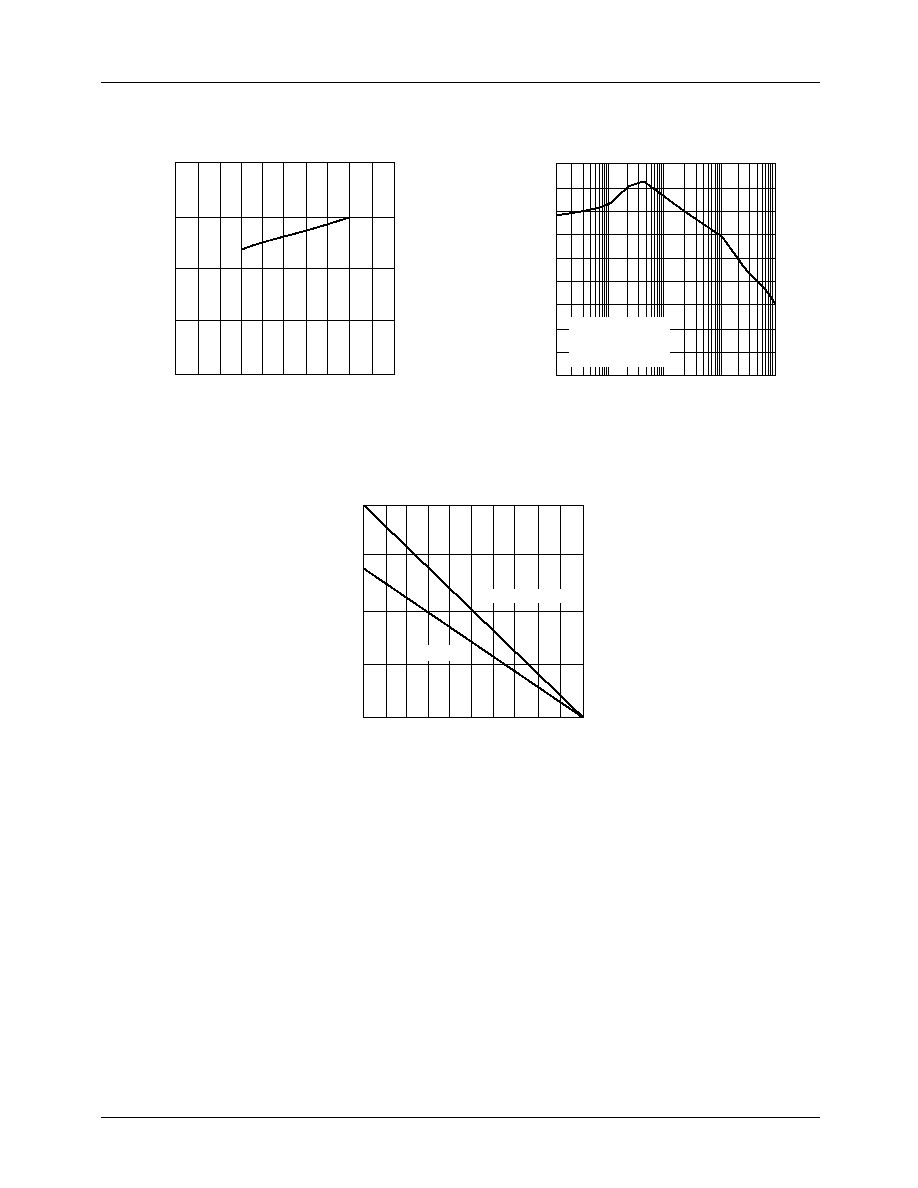
Typical Performance Characteristics
1.5
0.10
0.05
0
-0.05
-0.10
-0.15
-0.20
1.4
1.3
1.2
1.1
1.0
0.9
0.8
0.7
0.6
0.5
1.250
1.245
1.240
1.235
1.230
1.225
1.220
1.215
1.210
1.205
1.200
0
0
0.6
0.8
0.4
0.2
OUTPUT CURRENT (A)
JUNCTION TEMPERATURE (
∞
C)
JUNCTION TEMPERATURE (
∞
C)
JUNCTION TEMPERATURE (
∞
C)
DR
OPOUT V
O
L
T
A
GE
(V)
REFERENCE V
O
L
T
A
GE
(V)
3.70
3.65
3.60
3.55
3.50
3.45
3.40
3.35
3.30
3.25
3.20
REFERENCE V
O
L
T
A
GE
(V)
100
90
80
70
60
50
40
30
20
10
0
ADJUST PIN CURRENT (
µ
A)
5
4
3
2
1
0
MINIMUM LO
AD CURRENT (mA)
DR
OPOUT
V
O
L
T
A
GE DEVIA
TION (%)
1.0
-75 -50 -25 0
25 50 75 100 125 150 175
-75 -50 -25 0
25 50 75 100 125 150 175
-75 -50 -25 0
25 50 75 100 125 150 175
JUNCTION TEMPERATURE (
∞
C)
-75 -50 -25 0
25 50 75 100 125 150 175
JUNCTION TEMPERATURE (
∞
C)
-75 -50 -25 0
25 50 75 100 125 150 175
T
J
= 125
∞
C
T
J
= 0
∞
C
T
J
= 25
∞
C
I = 1A
V
OUT
= 3.6V
1
V
OUT
SET WITH 1% RESISTORS
V
OUT
= 3.3V
Note:
1. RC1117 Only
Note:
1. RC1117 Only
Figure 1. Dropout Voltage vs. Output Current
Figure 2. Load Regulation vs. Temperature
Figure 3. Reference Voltage vs. Temperature
Figure 4. Output Voltage vs. Temperature
Figure 5. Minimum Load Current vs. Temperature
Figure 6. Adjust Pin Current vs. Temperature
RC1117
PRODUCT SPECIFICATION
REV. 1.3.2 10/16/03
5
Typical Performance Characteristics
(continued)
2.0
1.75
1.5
1.25
1.0
SHOR
T
-
CIRCUIT CURRENT (A)
JUNCTION TEMPERATURE (
∞
C)
-75 -50 -25 0
25 50 75 100 125 150 175
10
7.5
5
2.5
0
PO
WER (W)
CASE TEMPERATURE (
∞
C)
25
45
65
85
105
125
SOT-223
90
80
70
60
50
40
30
20
10
0
RIPPLE REJECTION (dB)
FREQUENCY (Hz)
10
100
1K
10K
100K
(V
IN
- V
OUT
) = 3V
0.5 < V
RIPPLE
< 2V
I
OUT
= 1A
TO-252 & TO-263
Figure 7. Short-Circuit Current vs. Temperature
Figure 8. Ripple Rejection vs. Frequency
Figure 9. Maximum Power Dissipation
PRODUCT SPECIFICATION
RC1117
6
REV. 1.3.2 10/16/03
Mechanical Dimensions
4-Lead SOT-223 Package
A
--
.071
Symbol
Inches
Min.
Max.
Min.
Max.
Millimeters
Notes
A1
--
.181
.033
B
.025
c
--
.090
E
.130
.148
e
H
.264
.287
.115
.124
.033
.041
--
10
∞
F
F
I
J
D
.248
.264
--
1.80
--
4.80
.840
.640
--
2.29
3.30
3.71
6.71
7.29
.012
--
.310
--
2.95
3.15
.840
1.04
--
10
∞
10
∞
16
∞
K
10
∞
16
∞
.0008
.0040
L
.0203
.1018
10
∞
16
∞
M
10
∞
16
∞
.010
.014
N
.250
.360
6.30
6.71
A
D
e
E
c
H
A1
B
I
J
K
L
M
N

RC1117
PRODUCT SPECIFICATION
REV. 1.3.2 10/16/03
7
Mechanical Dimensions
3-Lead TO-252 Package
D
D1
GAGE PLANE
NOTES: UNLESS OTHERWISE SPECIFIED
A)
ALL DIMENSIONS ARE IN MILLIMETERS.
B)
THIS PACKAGE CONFORMS TO JEDEC, TO-252,
ISSUE C. VARIATION AA & AB, DATED NOV. 1999.
C)
DIMENSIONING AND TOLERANCING PER
ASME Y14.5≠1994.
D)
HEAT SINK TOP EDGE COULD BE IN CHAMFERED
CORNERS OR EDGE PROTRUSION.
E)
DIMENSIONS L3, D, E1 & D1 TABLE:
OPTION AA OPTION AB
0.89 ≠ 1.27
1.52 ≠ 2.03
5.97 ≠ 6.22
5.33 ≠ 5.59
4.32 MIN
3.81 MIN
5.21 MIN
L3
D
E1
D1
4.57 MIN
0.51
SEATING PLANE
DETAIL A
(1.54)
1.78
1.40
0.61
0.48
10
∞
0
∞
0.127 MAX
(ROTATED ≠90
∞
SCALE 12X
E1
L3
1
1
2
3
1
2
3
4
3
4
6.73
6.35
1.02
0.84
6.25
6.00 MIN
6.50 MIN
4.80
2.38
2.18
0.58
0.48
0.10
B
10.41
9.40
SEE
DETAIL A
3.00 MIN
1.40 MIN
LAND PATTERN RECOMMENDATION
1.14
0.78
0.89
0.54
SEE
NOTE D
(0.59)
2.29
5.46
5.21
4.57
0.25
A
C
M
M
2.90
2.30
C
A
B
PRODUCT SPECIFICATION
RC1117
8
REV. 1.3.2 10/16/03
Mechanical Dimensions
3-Lead TO-263 Package
A
.160
.190
4.06
4.83
Symbol
Inches
Min.
Max.
Min.
Max.
Millimeters
Notes
b
.020
.036
0.51
0.91
b2
.049
.051
1.25
1.30
c2
.045
.055
1.14
1.40
D
.340
.380
8.64
9.65
.380
.405
9.65
10.29
.100 BSC
E
e
L
.575
.625
14.61
15.88
.090
.110
2.29
2.79
L1
L2
--
.055
--
1.40
.017
.019
0.43
0.78
R
0
∞
8
∞
0
∞
8
∞
Notes:
1. Dimensions are exclusive of mold flash and metal burrs.
2. Standoff-height is measured from lead tip with ref. to Datum -B-.
3. Foot length is measured with ref. to Datum -A- with lead surface
(at inner R).
4. Dimensiuon exclusive of dambar protrusion or intrusion.
5. Formed leads to be planar with respect to one another at seating
place -C-.
2.54 BSC
E
@PKG/
@HEATSINK
D
L2
A
-C-
L
c2
L1
R (2 PLCS)
-A-
-B-
E-PIN
b2
b
e
PRODUCT SPECIFICATION
RC1117
LIFE SUPPORT POLICY
FAIRCHILD'S PRODUCTS ARE NOT AUTHORIZED FOR USE AS CRITICAL COMPONENTS IN LIFE SUPPORT DEVICES
OR SYSTEMS WITHOUT THE EXPRESS WRITTEN APPROVAL OF THE PRESIDENT OF FAIRCHILD SEMICONDUCTOR
CORPORATION. As used herein:
1. Life support devices or systems are devices or systems
which, (a) are intended for surgical implant into the body,
or (b) support or sustain life, and (c) whose failure to
perform when properly used in accordance with
instructions for use provided in the labeling, can be
reasonably expected to result in a significant injury of the
user.
2. A critical component in any component of a life support
device or system whose failure to perform can be
reasonably expected to cause the failure of the life support
device or system, or to affect its safety or effectiveness.
www.fairchildsemi.com
10/16/03 0.0m 005
Stock#DS30001117
2001 Fairchild Semiconductor Corporation
DISCLAIMER
FAIRCHILD SEMICONDUCTOR RESERVES THE RIGHT TO MAKE CHANGES WITHOUT FURTHER NOTICE TO
ANY PRODUCTS HEREIN TO IMPROVE RELIABILITY, FUNCTION OR DESIGN. FAIRCHILD DOES NOT ASSUME
ANY LIABILITY ARISING OUT OF THE APPLICATION OR USE OF ANY PRODUCT OR CIRCUIT DESCRIBED HEREIN;
NEITHER DOES IT CONVEY ANY LICENSE UNDER ITS PATENT RIGHTS, NOR THE RIGHTS OF OTHERS.
Ordering Information
Product Number
Output
Package
RC1117DT
Adjustable
TO-252 in tape and reel
RC1117M
Adjustable
TO-263
RC1117MT
Adjustable
TO-263 in tape and reel
RC1117ST
Adjustable
SOT-223 in tape and reel
RC1117D25T
2.5 volt
TO-252 in tape and reel
RC1117M25
2.5 volt
TO-263
RC1117M25T
2.5 volt
TO-263 in tape and reel
RC1117S25T
2.5 volt
SOT-223 in tape and reel
RC1117M285
2.85 volt
TO-263
RC1117M285T
2.85 volt
TO-263 in tape and reel
RC1117S285T
2.85 volt
SOT-223 in tape and reel
RC1117D33T
3.3 volt
TO-252 in tape and reel
RC1117M33
3.3 volt
TO-263
RC1117M33T
3.3 volt
TO-263 in tape and reel
RC1117S33T
3.3 volt
SOT-223 in tape and reel
RC1117D5T
5 volt
TO-252 in tape and reel
RC1117M5
5 volt
TO-263
RC1117M5T
5 volt
TO-263 in tape and reel
RC1117S5T
5 volt
SOT-223 in tape and reel