 | –≠–ª–µ–∫—Ç—Ä–æ–Ω–Ω—ã–π –∫–æ–º–ø–æ–Ω–µ–Ω—Ç: RC2798G | –°–∫–∞—á–∞—Ç—å:  PDF PDF  ZIP ZIP |
Document Outline
- Main Menu
- Selection Guide
- Special Function ICs
- Integrated QAM IF Downconverter
- Search
- fairchildsemi.com

PRELIMINARY INFORMATION describes products that are not in full production at the time of printing. Specifications are based on design goals
and limited characterization. They may change without notice. Contact Fairchild Semiconductor for current information.
www.fairchildsemi.com
Features
∑ RF input frequency range 30 to 250MHz
∑ On chip VCO with LO frequency range 30 to 250MHz
∑ IF amplifier with AGC setting
∑ High dynamic range -9dBm IIP3
∑ On chip Video Amplifier
∑ Built in ESD protection
∑ Supply voltage range 5 to 10 V
∑ Space saving 20-Lead TSSOP package
Applications
∑ Digital Set-top receivers
∑ Cable modems
∑ Internet surfboards
∑ Network Interface Modules
∑ Multimedia PCs
Description
The RC2798 is an integrated solution for the down-
conversion of QAM IF signals in the front-end design of
cable modem and set-top receivers. It is intended for use in
64QAM and 256QAM IF downconversion applications.
The RC2798 integrates IF amplifier with AGC , mixer, VCO,
and a video amplifier on a single chip. It accepts the QAM IF
signals via SAW filter and downconverts it to 5MHz
baseband signal.
The baseband signal can be digitized using Fairchild
Semiconductor's 8 bit A/D (TMC1175 series) or 10bit A/D
(TMC1185 series) and decoded further with a QAM
demodulator. The IF, Oscillator and Mixer section work at
5V. The video amplifier works at 5V to 10V. The RC2798 is
available in a 20 Lead TSSOP package.
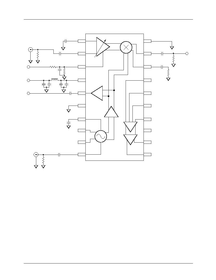
Block Diagram
1
AGC_IN1
2
AGC_IN2
3
VAGC
4
VCC MIX
5
OSC_OUT
6
GND
7
B2
8
C1
9
C2
10
20
19
18
17
16
15
14
13
12
11
B1
GND
MIX_OUT2
MIX_OUT1
G1A
G1B
VampIn1
VampIn2
VccAmp
VideoAmp
LO
AGC + MIX
RC2798
OUT1
OUT2
RC2798
Integrated QAM IF Downconverter
Rev 1.0.0

RC2798
PRODUCT SPECIFICATION
2
Absolute Maximum Ratings
(T
A
= 25
∞
C unless otherwise specified)
Notes:
1. Mounted on 50 X 50 X 1.6mm double epoxy glasss board.
Recommended Operating Range
Notes:
1. @ Vcc_Mix = VccVamp = 4.5 to 5.5V
2. @ Vcc_Mix = 4.5 to 5.5V, VccVamp = 4.5 to 10.0V
Parameter
Test conditions
Min.
Typ.
Max.
Unit
Video Amplifier 5V Operation
Vcc_Mix
Supply voltage 1 (for AGC amplifier,
oscillator, and mixer)
AGC amplifier, oscillator,
and mixer block
6
V
VccVamp
Supply voltage 2 ( for video
amplifier)
Video amplifier block
6
V
P
D
Power dissipation
T
A
= 85
∞
C
1
430
mW
T
A
Operation temperature range
-40
+85
∞
C
Tstg
Storage temperature range
-55
+150
∞
C
Video Amplifier 9V Operation
Vcc_Mix
Supply voltage 1 (for AGC amplifier,
oscillator, and mixer)
AGC amplifier, oscillator,
and mixer block
6
V
VccVamp
Supply voltage 2 ( for video
amplifier)
Video amplifier block
11
V
P
D
Power dissipation
T
A
= 75
∞
C
1
500
mW
T
A
Operation temperature range
-40
+75
∞
C
Tstg
Storage temperature range
-55
+150
∞
C
Parameter
Min.
Typ. Max.
Unit
Vcc_Mix
Supply voltage 1 (for AGC amplifier, oscillator,
and mixer)
4.5
5.0
5.5
V
VccVamp
Supply voltage 2 ( for video amplifier)
4.5
5.0
10.0
V
Ta1
Operation temperature range 1
1
-40 +25
+85
∞
C
Ta2
Operation temperature range 2
2
-40
+25
+75
∞
C

PRODUCT SPECIFICATION
RC2798
3
Electrical Characteristics
(T
A
= 25
∞
C )
Standard Characteristics
(V
CC
= 5V, T
A
= 25
∞
C)
Parameter
Test conditions
Min.
Typ.
Max.
Unit
AGC Amplifier, Oscillator, and Mixer Blocks (Vcc = 5V)
Icc1
Supply current 1
no input signal
17.0
23.0
31.0
mA
f
RF
RF input frequency range
30
250
MHz
f
OSC
OSC frequency range
30
250
MHz
f
IF
IF output frequency range
DC
150
MHz
CG
MAX
Maximum conversion gain
V
AGC
= 4.0V
25
dB
CG
MIN
Minimum conversion gain
V
AGC
= 1.0V
-7
dB
GCR
AGC dynamic range
V
AGC
= 1.0 to 4.0V
24
32
40
dB
NF
Noise figure
SSB, V
AGC
= 4.0V
At maximum gain
9
dB
V
AGC
H
AGC voltage high level
At maximum gain
4.0
V
V
AGC
L
AGC voltage low level
At minimum gain
1.0
V
Video Amplifier Block (Vcc = 5V)
Icc2
Supply current 2
No input signal
7.0
12.5
17.0
mA
V
OUT
Output voltage
RL = 1K
W
, differential
3.0
Vp-p
G1
Differential gain 1
G1A-G1B pins: short,
V
OUT
= 3Vp-p
150 200
250
V/V
G2
Differential gain 2
G1A-G1B pins: open,
V
OUT
= 3Vp-p
22.0 26.0
30.0
V/V
Video Amplifier Block (Vcc = 9V)
Icc2
Supply current 2
no input signal
18.0
24.0
32.0
mA
V
OUT
Output voltage
RL = 1K
W
, differential
3.0
Vp-p
G1
Differential gain 1
G1A-G1B pins: short,
RL = 2K
W
300
385
470
V/V
G2
Differential gain 2
G1A-G1B pins: open,
RL = 2K
W
25.0
28.5
32.0
V/V
Video Amplifier Block (Vcc = 5V or 9V)
BW
G1
Bandwidth 1
G1
50
MHz
BW
G2
Bandwidth 2
G2
50
MHz
Rin1
Input resistance 1
G1
3.5
K
W
Rin2
Input resistance 2
G2
7.5
K
W
Cin
Input capacitance
1.6
pF
Parameter
Test conditions
Min.
Typ.
Max.
Unit
AGC Amplifier Block (Vcc = 5V)
AGC IIP3
AGC input intercept point
At minimum gain
(AGC amplifier + mixer)
-9
dBm
Video Amplifier Block (Vcc = 5V or 9V)
CMRR
Common mode rejection ratio
80
dB
PSRR
Power supply rejection ratio
70
dB
t
r
Rise time
2.6
nS
t
PD
Propagation delay time
4.4
nS

RC2798
PRODUCT SPECIFICATION
4
Typical Characteristics
Figure 1. AGC Control Characteristics
Figure 2. Supply Current vs. Supply Voltage
-10
-5
0
5
10
15
20
25
30
0
5.00
E-01
1
1.5
2
2.5
3
3.5
4
4.5
5
AGC control ≠ Volts
Conversion gain ≠ dB
Series1
conv. gain
-5.00E-03
0.00E+00
5.00E-03
1.00E-02
1.50E-02
2.00E-02
2.50E-02
3.00E-02
3.50E-02
4.00E-02
4.50E-02
0
4.00
E-01
8.00
E-01
1.2
1.6
2
2.4
2.8
3.2
3.6
4
4.4
4.8
5.2
5.6
6
Supply voltage ≠ Volts
Supply current ≠ A
Total
AGC amp + Mixer + LO
Video Amp
PRODUCT SPECIFICATION
RC2798
5
Figure 3. Measurement Circuit 1--AGC + MIX Block
1
AGC_IN1
10nF
10nF
10nF
10nF
10nF
1K
1K
10nF
10nF
0.22
µ
F
FB
10
µ
F
10
µ
F
0.1
µ
F
0.1
µ
F
+
+
10K
51
RF input
VAGC (1.0≠4.0V)
Vcc_Mix(+5V)
Oscillator O/P
Ext. LO I/P
10K
2
AGC_IN2
3
VAGC
4
VCC MIX
5
OSC_OUT
6
GND
7
B2
51
8
C1
9
C2
10
20
19
18
17
16
15
14
13
12
11
B1
GND
MIX_OUT2
MIX OUT
MIX_OUT1
G1A
G1B
VampIn1
VampIn2
VccAmp
VideoAmp
LO
AGC + MIX
RC2798
OUT1
OUT2