 | –≠–ª–µ–∫—Ç—Ä–æ–Ω–Ω—ã–π –∫–æ–º–ø–æ–Ω–µ–Ω—Ç: RC4157 | –°–∫–∞—á–∞—Ç—å:  PDF PDF  ZIP ZIP |
www.fairchildsemi.com
REV. 1.0.1 6/13/01
Features
∑ Unity gain bandwidth for RC4156 ≠ 3.5 MHz
∑ Unity gain bandwidth for RC4157 ≠ 19 MHz
∑ High slew rate for RC4156 ≠ 1.6 V/µS
∑ High slew rate for RC4157 ≠ 8.0V/µS
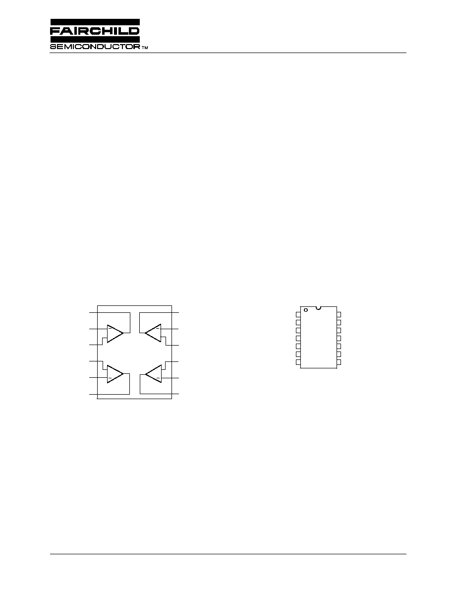
Block Diagram
A
D
C
B
65-3463-01
Output (A)
≠Input (A)
+Input (A)
+Input (B)
≠Input (B)
Output (B)
Output (D)
≠Input (D)
+Input (D)
+Input (C)
≠Input (C)
Output (C)
+
+
+
+
∑ Low noise voltage ≠ 1.4 µVRMS
∑ Indefinite short circuit protection
∑ No crossover distortion
Description
The RC4156 and RC4157 are monolithic integrated circuits,
consisting of four independent high performance operational
amplifiers constructed with an advanced epitaxial process.
These amplifiers feature improved AC performance which
far exceeds that of the 741 type amplifiers. Also featured are
excellent input characteristics and low noise, making this
device the optimum choice for audio, active filter and instru-
mentation applications. The RC4157 is a decompensated
version of the RC4156 and is AC stable in gain configura-
tions of -5 or greater.
Pin Assignments
1
2
3
4
5
6
7
14
13
12
11
10
9
8
Output (A)
≠Input (A)
+Input (A)
+VS
+Input (B)
≠Input (B)
Output (B)
Output (D)
≠Input (D)
+Input (D)
≠VS
+Input (C)
≠Input (C)
Output (C)
65-3463-02
RC4156/RC4157
High Performance Quad Operational Amplifiers

PRODUCT SPECIFICATION
RC4156/RC4157
2
REV. 1.0.1 6/13/01
Absolute Maximum Ratings
(beyond which the device may be damaged)1
Notes:
1. Functional operation under any of these conditions is NOT implied. Performance and reliability are guaranteed only if
Operating Conditions are not exceeded.
2. For supply voltages less than ±15V, the absolute maximum input voltage is equal to the supply voltage.
3. Short circuit to ground on one amplifier only.
Operating Conditions
Electrical Characteristics
(V
S
= ±15V, RC = 0∞C
T
A
+70∞C)
Parameter
Min
Typ
Max
Units
Supply Voltage
±20
V
Input Voltage
2
±15
V
Differential Input Voltage
30
V
Output Short Circuit Duration
3
Indefinite
P
D
T
A
< 50∞C
SOIC
300
mW
PDIP
468
mW
Operating Temperature
RC4156/RC4157
0
70
∞C
Storage Temperature
-65
150
∞C
Junction Temperature
SOIC, PDIP
125
∞C
Lead Soldering Temperature
(60 seconds)
DIP
300
∞C
SOIC
260
∞C
For T
A
> 50∞C Derate at
SOIC
5.0
mW/∞C
PDIP
6.25
mW/∞C
Parameter
Min
Typ
Max
Units
JC
Thermal resistance
60
∞C/W
JA
Thermal resistance
SOIC
200
∞C/W
PDIP
160
∞C/W
RC4156/4157
Parameters
Test Conditions
Min
Typ
Max
Units
Input Offset Voltage
R
S
10 k
6.5
mV
Input Offset Current
100
nA
Input Bias Current
400
nA
Large Signal Voltage Gain
R
L
2 k,V
OUT
±10V
15
V/mV
Output Voltage Swing
R
L
2 k
±10
V
Supply Current
10
mA
Average Input Offset Voltage Drift
5.0
µV/∞C

RC4156/RC4157
PRODUCT SPECIFICATION
REV. 1.0.1 6/13/01
3
Electrical Characteristics
(V
S
= ±15V and T
A
= +25∞C unless otherwise noted)
Note:
1. Sample tested only.
RC4156/4157
Units
Parameters
Test Conditions
Min
Typ
Max
Input Offset Voltage
R
S
10 k
1.0
5.0
mV
Input Offset Current
30
50
nA
Input Bias Current
60
300
nA
Input Resistance
0.5
M
Large Signal Voltage Gain
R
L
2 k, V
OUT
±10V
25
100
V/mV
Output Voltage Swing
R
L
10 k
±12
±14
V
R
L
2 k
±10
±13
V
Input Voltage Range
±12
±14
V
Output Resistance
230
Short Circuit Current
25
mA
Common Mode Rejection Ratio
R
S
10 k
80
dB
Power Supply Rejection Ratio
R
S
10 k
80
dB
Supply Current (All Amplifiers)
R
L
=
5.0
7.0
mA
Transient Response (4156)
Rise Time
60
nS
Overshoot
25
%
Slew Rate
1.3
1.6
V/µS
Unity Gain Bandwidth (4156)
2.8
3.5
MHz
Phase Margin (4156)
R
L
= 2 k
, C
L
= 50 pF
50
%
Transient Response (4157)
A
V
= -5
Rise Time
50
nS
Overshoot
25
%
Slew Rate
6.5
8.0
V/µS
Unity Gain Bandwidth (4157)
A
V
= -5
15
19
MHz
Phase Margin (4157)
A
V
= -5, R
L
= 2 k
,
C
L
= 50 pF
50
%
Power Bandwidth
V
OUT
= 20V
p-p
20
25
kHz
Input Noise Voltage
1
F = 20 Hz to 20 kHz
1.4
5.0
µV
RMS
Input Noise Current
F = 20 Hz to 20 kHz
15
pA
RMS
Channel Separation
108
dB

PRODUCT SPECIFICATION
RC4156/RC4157
4
REV. 1.0.1 6/13/01
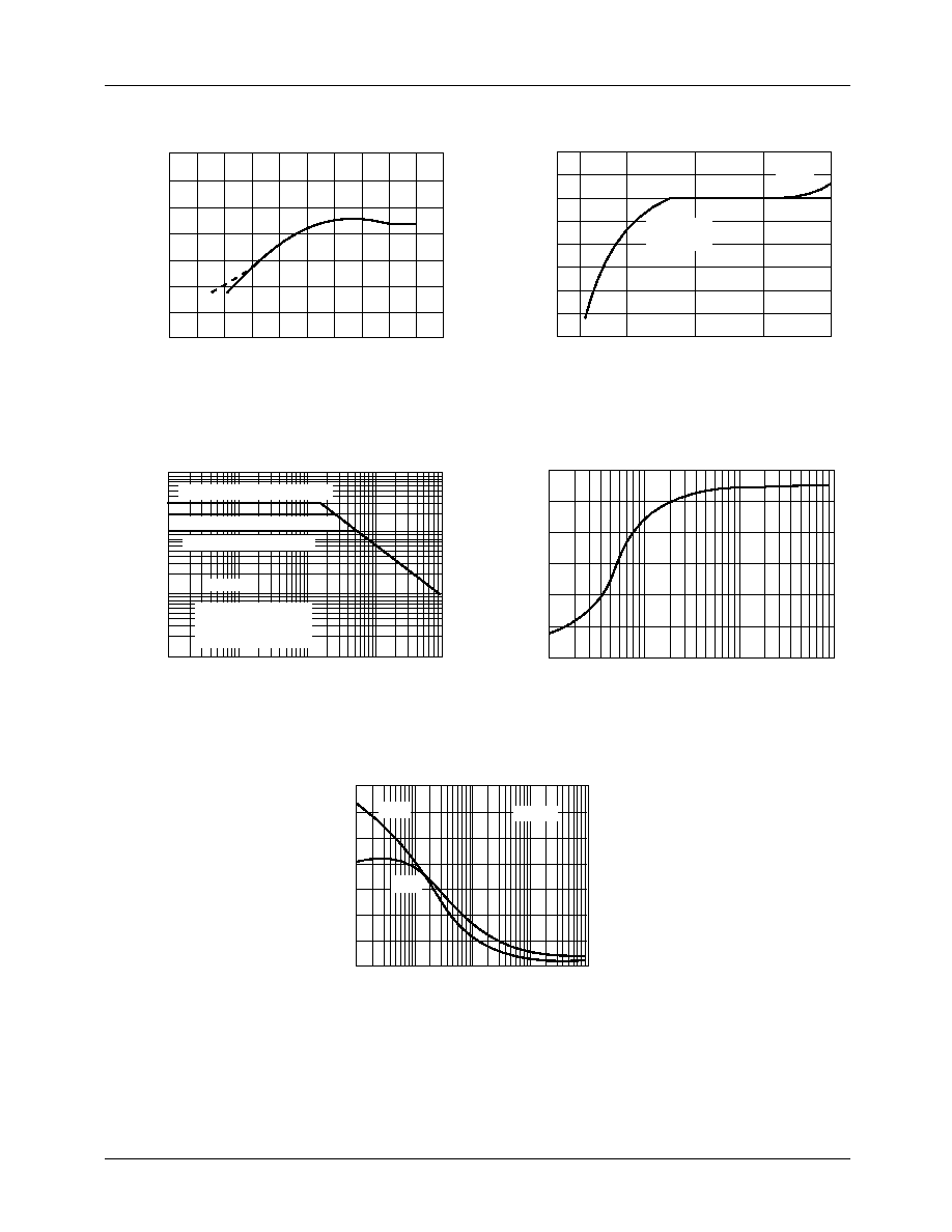
Typical Performance Characteristics
Figure 1. Open Loop Gain, Phase vs. Frequency
Figure 2. PSRR vs. Temperature
Figure 3. Channel Separation vs. Frequency
Figure 4. Transient Response vs. Temperature
Figure 5. Input Noise Voltage, Current
Density vs. Frequency
A
VOL
(dB)
(Deg)
F (Hz)
65-0738
110
100
90
80
70
60
50
40
30
20
10
0
-10
1
10
100
1K
10K 100K 1M
10M
0
45
90
135
180
4156
A
VOL
R = 2K
C = 55 pF
L
L
PSRR (dB)
T
A
(
∞C)
65-0740
140
120
100
80
60
40
20
0
-100
-50
0
+50
+100
+150
-25
+25
+75
+125
-75
+V
S
-V
S
100K
1K
1K
V
OUT1
100K
1K
1K
V
OUT2
C.S. = 20 log ( )
V
100 V
OUT2
OUT1
65-0739
CS (dB)
F (Hz)
-140
-120
-100
-80
-60
-40
-20
0
10
100
1K
10K
100K
3
2
1
5
6
7
4156/57
4156/57
Transient Response
(Normalized to +25
∞
C)
T
A
(
∞C)
65-0741
1.3
1.2
1.1
1.0
0.9
0.8
0.7
0.6
-100
-50
0
+50
+100
+150
-75
-25
+25
+75
+125
65-0742
1.4
1.2
1.0
0.8
0.6
0.4
0.2
0
35
30
25
20
15
10
5
0
10
100
1K
10K
100K
e
n
I
N
F (Hz)
e
n
(nV Hz )
I
N
(pA Hz )
RC4156/RC4157
PRODUCT SPECIFICATION
REV. 1.0.1 6/13/01
5
Typical Performance Characteristics
(continued)
Figure 6. Slew Rate, Bandwidth vs. Temperature
Figure 7. Slew Rate, Bandwidth vs. Supply Voltage
Figure 8. Output Voltage Swing vs. Frequency
Figure 9. Output Voltage Swing vs. Load Resistance
Figure 10. Small Signal Phase Margin,
Unity Gain Bandwidth vs. Load Capacitance
65-0743
SR,BW
(Normalized to +25
∞
C)
T
A
(
∞C)
1.3
1.2
1.1
1.0
0.9
0.8
0.7
0.6
-100
-50
0
+50
+100
+150
65-0744
±V
S
(V)
SR, BW
(Normalized to
±
15V)
1.1
1.0
0.9
0.8
0.7
0
±2
±5
±10
±15
±20
BW
SR and
BW
65-0746
F (Hz)
V
OUT P-P
(V)
4156
(Voltage Follower)
R = Open
C = 50 pF
L
L
10
1.0
0.1
30
100
1K
10K
100K
1M
V
OUT P-P
= 28V V
S
=
±15V
V
OUT P-P
= 18V V
S
=
±10V
V
OUT P-P
= 8V V
S
=
±5V
65-0749
R
L
( )
V
OUT P-P
(V)
30
25
20
15
10
05
0
100
1K
10K
100K
65-0745
M (Deg)
C
L
(pF)
BW (MHz)
70
60
50
40
30
20
10
0
10
100
1K
10K
100K
7
6
5
4
3
2
1
0
M
BW
4156