 | –≠–ª–µ–∫—Ç—Ä–æ–Ω–Ω—ã–π –∫–æ–º–ø–æ–Ω–µ–Ω—Ç: RC4194 | –°–∫–∞—á–∞—Ç—å:  PDF PDF  ZIP ZIP |
Document Outline
- Main Menu
- Analog & Mixed Signal
- Regulators PSG
- Regulators Index
- Search
- fairchildsemi.com
www.fairchildsemi.com
Features
∑ Simultaneously adjustable outputs with one resistor
to
±42V
∑ Load current ≠
±200 mA with 0.04% load regulation
Description
The RC/RM4194 are dual polarity tracking regulators
designed to provide balanced or unbalanced positive and
negative output voltages at currents to 200 mA.
A single external resistor adjustment can be used to change
both outputs between the limits of
±50 mV and ±42V.
These devices are designed for local "on-card" regulation,
eliminating distribution problems associated with single-
point regulation. To simplify application the regulators
require a minimum number of external parts.
The device is available in three package types to accommo-
date various power requirements. The K (TO-66) power
package can dissipate up to 3W at T
A
= +25
∞C. The D
14-pin dual in-line will dissipate up to 1W and the N
14-pin dual in-line will dissipate up to 625 mW.
∑ Internal thermal shutdown at T
J
= +175
∞C
∑ External balance for
±V
OUT
unbalancing
∑ 3W power dissipations
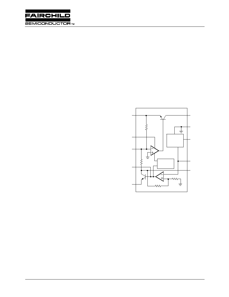
Block Diagram
Comp+
Bal
+V
S
≠V
S
≠V
OUT
+V
OUT
GND
R
SET
R
O
65-4194-01
Thermal
Shutdown
100
µ
A
Current
Source
Comp≠
20K
4194
20K
3R
R
RC4194
Dual Tracking Voltage Regulators
Rev. 1.0.0
PRODUCT SPECIFICATION
RC4194
2
Absolute Maximum Ratings
(beyond which the device may be damaged)1
Note:
1. Functional operation under any of these conditions is NOT implied.
Parameter
Min
Typ
Max
Units
Supply Voltage
RC4194
±
35
V
RM4194
±
45
V
Supply Input to Output Voltage Differential
RC4194
±
35
V
RM4194
±
45
V
Load Current
PDIP
100
mA
CerDIP
150
mA
TO-66 Metal Can
250
mA
P
D
T
A
< 50
∞
C
PDIP
468
mW
CerDIP
1042
mW
TO-66 Metal Can
2381
mW
Operating Temperature (T
j
)
RC4194
0
70
∞
C
RM4194
-55
125
∞
C
Storage Temperature
-65
150
∞
C
Junction Temperature
PDIP
125
∞
C
CerDIP
175
∞
C
TO-66 Metal Can
150
∞
C
Lead Soldering Temperature (60 seconds)
300
∞
C
For T
A
> 50
∞
C Derate at
TO-66 Metal Can
23.81
mW/
∞
C
PDIP
6.25
mW/
∞
C
CerDIP
8.38
mW/
∞
C
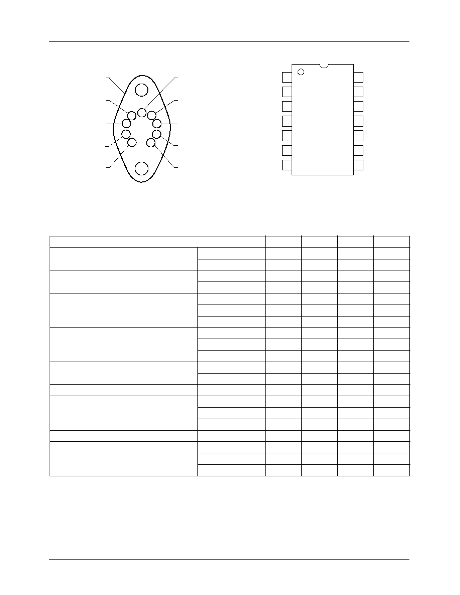
Pin Assignments
65-4194-02
1
9
2
3
4
5
6
7
8
+V
GND
R
R
-V
OUT
Comp-
Bal
Comp+
+V
OUT
-V (Case)
S
SET
O
S
1
2
3
4
5
6
7
8
9
10
11
12
13
14
NC
Comp+
Bal
Comp-
NC
S
+V
OUT
-V
+V
NC
GND
R
R
NC
-V
OUT
S
SET
O
65-4194-03

RC4194
PRODUCT SPECIFICATION
3
Operating Conditions
Electrical Characteristics
(
±
5
£
V
OUT
£
V
MAX
; ≠V
IN
£
-8V; I
L
=
±
1mA; RM4194: -55
∞
C
£
T
j
£
+125
∞
C; RC4194: 0
∞
C
£
T
j
£
+70
∞
C
unless otherwise specified)
Notes:
1. Measured as
(mA)
2. Output voltage temperature drift guaranteed by design.
3. The current drain will increase by 50
m
A/V
OUT
on positive side and 100
m
A/V
OUT
on negative side.
4. The specifications above apply for the given junction temperatures since pulse test conditions are used.
Parameter
Min
Typ
Max
Units
q
JC
Thermal Resistance
CerDIP
60
∞
C/W
TO-66 Metal Can
7
∞
C/W
q
JA
Thermal Resistance
PDIP
160
∞
C/W
CerDIP
120
∞
C/W
TO-66 Metal Can
42
∞
C/W
Parameters
Test Conditions
Min
Typ
Max
Units
Line Regulation
D
V
S
= 0.1 V
IN
0.04
0.1
%V
OUT
Load Regulation
1
4194K: I
L
< 200 mA
4194D: I
L
< 100 mA
±
V
S
=
±
(V
OUT
+ 5)V
0.002
0.004
%V
OUT
/I
L
(mA)
Output Voltage Drift With
Temperature
2
Positive Output
V
OUT
=
±
5V
0.002
0.015
%/
∞
C
Negative Output
V
OUT
=
±
5V
0.003
0.015
%/
∞
C
Supply Current
3
(Positive)
V
S
=
±
V
MAX
, V
OUT
= 0V,
I
L
= 0 mA
+0.8
+2.5
mA
Supply Current
4
(Negative)
V
S
=
±
V
MAX
, V
OUT
= 0V,
I
L
= 0 mA
-1.8
-4.0
mA
Supply Voltage
RM4194
±
9.5
±
45
V
RC4194
±
9.5
±
35
V
Output Voltage Scale Factor
R
SET
= 71.5 k
W
, T
j
= +25
∞
C,
V
S
=
±
V
MAX
2.38
2.5
2.62
k
W
/V
Output Voltage Range
RM4194: R
SET
= 71.5 k
W
,
I
L
= 25 mA
0.05
±
42
V
RC4194: R
SET
= 71.5 k
W
,
I
L
= 25 mA
0.05
±
42
V
Output Voltage Tracking
±
0.4
±
2.0
%
Ripple Rejection
F = 120 Hz, T
j
= +25
∞
C
70
dB
Input-Output Voltage Differential
I
L
= 50 mA, T
j
= +25
∞
C
3.0
V
Short Circuit Current
V
S
=
±
30V, T
j
= +25
∞
C
300
mA
Output Noise Voltage
C
L
= 4.7
m
F, V
OUT
=
±
15V,
F = 10 Hz to 100 kHz
250
m
V
RMS
Internal Thermal Shutdown
175
∞
C
D
V
OUT
V
OUT
------------------
100%
¥
Ë
¯
Ê
ˆ
I
L
ß
PRODUCT SPECIFICATION
RC4194
4
Typical Performance Characteristics
Figure 1. Ripple Rejection vs. Frequency
Figure 2. Load Regulation vs. Load Current
Figure 3. Output Voltage Tracking vs. Temperature
65-0201
Ripple Rejection (dB)
F (Hz)
150
130
110
90
70
50
30
10
0
100
1K
10K
100K
V
OUT
=
±
15V
65-0202
T
j
= +125
°
C
T
j
= +25
°
C
0.06
0.05
0.04
0.03
0.02
0.01
0
-0.01
0
20
40
60
80 100 120 140 160 180 200
I
L
(mA)
Load Regulation (% V
OUT
/I
L
)
65-0203
0.8
0.6
0.4
0.2
0
-0.2
-0.4
-0.6
T
j
(
°
C)
Output Voltage Tracking (% V
OUT
)
A
B
C
-60
-40 -20
0
+20 +40 +60 +80 +100+120+140
A = % Tracking of V
OUT
B = T.C. for Positive Regulator
C = T.C. for Negative Regulator

RC4194
PRODUCT SPECIFICATION
5
Typical Applications
Figure 4. Unbalanced Output Voltage -- Comparator Application
Figure 5. High Output Application
0.01
µ
F
S
-V
S
+V
S
+V
-V
S
71.5K
0.01
µ
F
R
SET
Comp-
Gnd
RM4194
Comp+
R
-V
Bal
+V
OUT
OUT
0
0
R
A
R
B
R
4.7
µ
F
4805
4.7
µ
F**
+V
OUT
To Additional
Comparators
(Typically 15 RC4805s)
-V = -5V
To Additional
Comparators
R (k
Ω
) = 2.5 (-V )
Adjust R for -V = -5V (12.5 k )
R = R = 20 k
Ω
(See Schematic)
+ V = -V
R = when +V -V
R = when +V -V
For +V = 5 when -V = -5V
R =
R =
W
OUT
OUT
O
O
F1
F2
OUT
OUT
A
OUT
OUT
B
OUT
OUT
OUT
OUT
A
B
OUT
R R
R R
F1
A
F2
B
65-0205
65-0206
S
+V
-V
S
0.1 F
m
+V
-V
GND
Comp+
-V
+V
R
Comp-
R
R
60
µ
F
-V
60
µ
F**
2N2297 or equiv.
R *
0.1 F
4194
71.5K
2N914 or equiv.
2N2297 or equiv.
R *
47
47
2N4905 or equiv.
*R =
**Optional usage - Not as critical as -V bypass capacitors.
Note: Compensation and bypass capacitor connections should be close as posibe to the 4194
0.7
I
SC
SC
O
SC
S
S
SET
OUT
OUT
SC
0
OUT
W
+V
OUT
0
m
W
Load regulation
10 mV @ 2.5A
R (k ) = 2.5 V
O
W
O