 | ÐлекÑÑоннÑй компоненÑ: RC4200AN | СкаÑаÑÑ:  PDF PDF  ZIP ZIP |
Äîêóìåíòàöèÿ è îïèñàíèÿ www.docs.chipfind.ru
www.fairchildsemi.com
REV. 1.2.1 6/14/01
Features
· High accuracy
· Nonlinearity 0.1%
Temperature coefficient 0.005%/°C
· Multiple functions
· Multiply, divide, square, square root, RMS-to-DC
conversion, AGC and modulate/demodulate
· Wide bandwidth 4 MHz
· Signal-to-noise ratio 94 dB
Applications
· Low distortion audio modulation circuits
· Voltage-controlled active filters
· Precision oscillators
Description
The RC4200 analog multiplier has complete compensation
for nonlinearity, the primary source of error and distortion.
This multiplier also has three onboard operational amplifiers
designed specifically for use in multiplier logging circuits.
These amplifiers are frequency compensated for optimum
AC response in a logging circuit, the heart of a multiplier,
and can therefore provide superior AC response.
The RC4200 can be used in a wide variety of applications
without sacrificing accuracy. Four-quadrant multiplication,
two-quadrant division, square rooting, squaring and RMS
conversion can all be easily implemented with predictable
accuracy. The nonlinearity compensation is not just trimmed
at a single temperature, it is designed to provide compensa-
tion over the full temperature range. This nonlinearity
compensation combined with the low gain and offset drift
inherent in a well-designed monolithic chip provides a very
high accuracy and a low temperature coefficient.
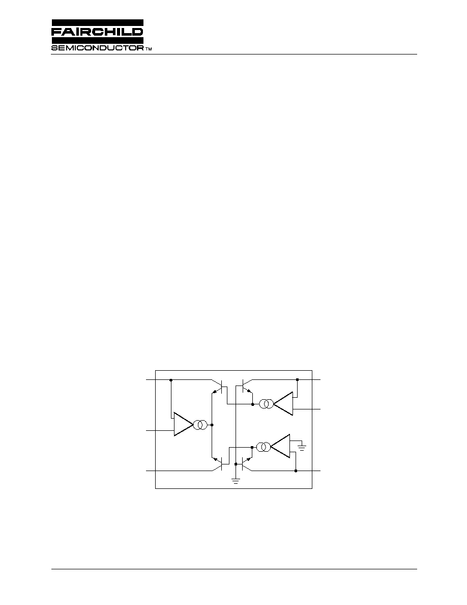
Block Diagram
65-4200-01
RC4200
I2
+
+
+
I3
V
OS2
V
OS1
Q3
Q4
I4
I1
Q1
Q2
RC4200
Analog Multiplier

RC4200
PRODUCT SPECIFICATION
2
REV. 1.2.1 6/14/01
Functional Description
The RC4200 multiplier is designed to multiply two input
currents (I
1
and I
2
) and to divide by a third input current (I
4
).
The output is also in the form of a current (I
3
). A simplified
circuit diagram is shown in the Block Diagram. The nominal
relationship between the three inputs and the output is:
The three input currents must be positive and restricted to a
range of 1 µA to 1 mA. These currents go into the multiplier
chip at op amp summing junctions which are nominally at
zero volts. Therefore, an input voltage can be easily
converted to an input current by a series resistor. Any
number of currents may be summed at the inputs. Depending
on the application, the output current can be converted to a
voltage by an external op amp or used directly. This capa-
bilty of combining input currents and voltages in various
combinations provides great versatility in application.
Inside the multiplier chip, the three op amps make the
collector currents of transistors Q1, Q2 and Q4 equal to their
respective input currents (I
1
, I
2
, and I
4
). These op amps are
designed with current source outputs and are phase-compen-
sated for optimum frequency response as a multiplier. Power
drain of the op amps was minimized to prevent the introduc-
tion of undesired thermal gradients on the chip. The three op
amps operate on a single supply voltage (nominally -15V)
and total quiescent current drain is less than 4 mA. These
special op amps provide significantly improved performance
in comparison to 741-type op amps.
The actual multiplication is done within the log-antilog
configuration of the Q1-Q4 transistor array. These four
transistors, with associated proprietary circuitry, were
specially designed to precisely implement the relationship.
I
3
I
1
I
2
I
4
--------- 1
( )
=
V
BEN
kT
Q
-------In
I
CN
I
SN
--------- 2
( )
=
Previous multiplier designs have suffered from an additional
undesired linear term in the above equation; the collector
current times the emitter resistance. The I
C
r
E
term intro-
duces a parabolic nonlinearity even with matched transistors.
Fairchild Semiconductor has developed a unique and propri-
etary means of inherently compensating for this undesired
I
C
r
E
term. Furthermore, this Fairchild Semiconductor devel-
oped circuit technique compensates linearity error over tem-
perature changes. The nonlinearity versus temperature is
significantly improved over earlier designs.
From equation (2) and by assuming equal transistor junction
temperatures, summing base-to-emitter voltage drops around
the transistor array yields:
This equation reduces to:
The rate of reverse saturation current I
S1
I
S2
/I
S3
I
S4
, depends
on the transistor matching. In a monolithic multiplier this
matching is easily achieved and the rate is very close to
unity, typically 1.0±1%. The final result is the desired
relationship:
The inherent linearity and gain stability combined with low
cost and versatility makes this new circuit ideal for a wide
range of nonlinear functions.
KT
q
-------- In
I
1
I
S1
-------
In
I
2
I
S2
-------
In
I
3
I
S3
------- In
I
4
I
S4
-------
=
0 3
( )
=
I
1
I
2
I
3
I
4
---------
I
S1
I
S2
I
S3
I
S4
--------------- 4
( )
=
I
3
I
1
I
2
I
4
--------- 5
( )
=
Pin Assignments
1
2
3
4
I2
VOS2
VS
I3 (Output)
I1
VOS1
GND
I4
8
7
6
5
65-4200-07
PRODUCT SPECIFICATION
RC4200
REV. 1.2.1 6/14/01
3
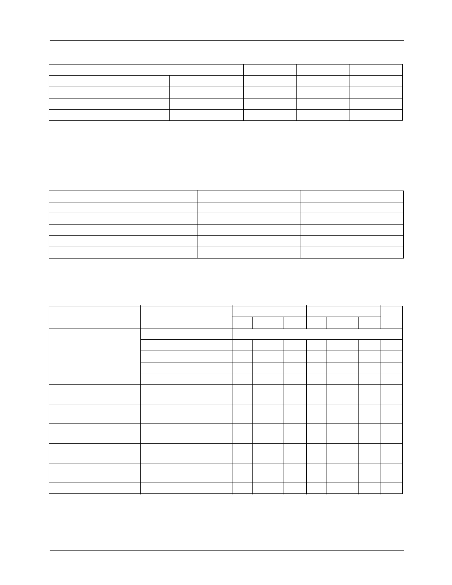
Absolute Maximum Ratings
Notes:
1. For a supply voltage greater than -22V, the absolute maximum input voltage is equal to the supply voltage.
2. Observe package thermal characteristics.
Thermal Characteristics
(Still air, soldered into PC board)
Parameter
Min.
Max.
Unit
Supply Voltage
1
-22
V
Input Current
-5
mA
Storage Temperature Range
RC4200/4200A
-55
+125
°C
Operating Temperature Range
RC4200/4200A
0
+70
°C
8-Lead Plastic DIP
8-Lead SOIC
Maximum Junction Temperature
+125°C
+125°C
Maximum P
D
T
A
< 50°C
468mW
300mW
Thermal Resistance
JC
--
--
Thermal Resistance
JA
160°C/W
240°C/W
For T
A
> 50°C Derate at
6.25mW/°C
4.17mW/°C
Electrical Characteristics
(Over operating temperature range, V
S
= -15V unless otherwise noted)
Parameters
Test Conditlons
4200A
4200
Min.
Typ.
Max. Min.
Typ.
Max. Units
Total Error as Multiplier
TA = +25°C
Untrimmed
1
±2.0
±3.0
%
With External Trim
±0.2
±0.2
%
Versus Temperature
±0.005
±0.005
%/°C
Versus Supply (-9 to -18V)
±0.1
±0.1
%/V
Nonlinearity
2
50µA
I
1,2,4
250 µA,
T
A
= +25°C
±0.1
±0.3
%
Input Current Range
(I
1
, I
2
and I
4
)
1.0
1000
1.0
1000
µA
Input Offset Voltage
I
1
= I
2
= I
4
= 150 µA
T
A
= +25°C
±5.0
±10
mV
Input Bias Current
I
1
= I
2
= I
4
= 150 µA
T
A
= +25°C
300
500
nA
Average Input Offset
Voltage Drift
I
1
= I
2
= I
4
= 150 µA
±50
±100 µV/°C
Output Current Range (I
3
)
3
1.0
1000
1.0
1000
µA
RC4200
PRODUCT SPECIFICATION
4
REV. 1.2.1 6/14/01
Notes:
1. Refer to Figure 6 for example.
2. The input circuits tend to become unstable at I
1
, I
2
, I
4
< 50 µA and linearity decreases when I
1
, I
2
, I
4
> 250 µA
(eq. @ I
1
= I
2
= 500 µA, nonlinearity error
0.5%).
3. These specifications apply with output (I
3
) connected to an op amp summing junction. If desired, the output (I
3
) at pin (4) can
be used to drive a resistive load directly. The resistive load should be less than 700
and must be pulled up to a positive
supply such that the voltage on pin (4) stays within a range of 0 to +5V.
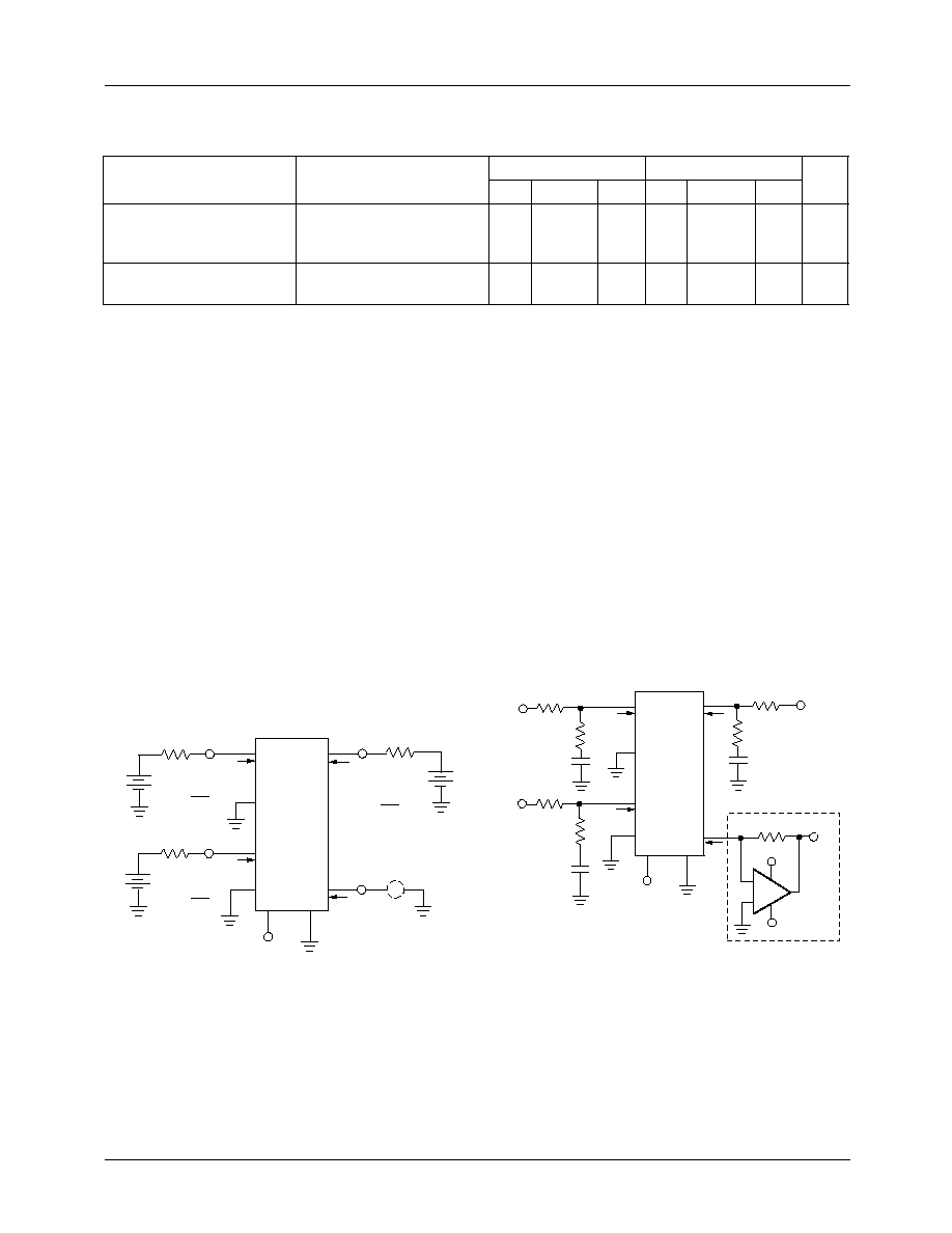
Frequency Response,
-3dB point
Supply Voltage
-18
4.0
-15
-9.0
-18
4.0
-15
-9.0
MHz
V
Supply Current
I
1
= I
2
= I
4
= 150 µA
T
A
= +25°C
4.0
4.0
mA
Electrical Characteristics
(continued)
(Over operating temperature range, V
S
= -15V unless otherwise noted)
Parameters
Test Conditlons
4200A
4200
Min.
Typ.
Max. Min.
Typ.
Max. Units
Applications Discussion
Current Multiplier/ Divider
The basic design criteria for all circuit configurations using
the RC4200 multiplier is contained in equation (1), that is,
The current-product-balance equation restates this as:
Figure 1. Current Multiplier/Divider
I
3
I
1
I
2
I
4
---------
=
I
1
I
2
I
3
I
4
6
( )
=
65-4200-02
RC4200
+V
Z
R
1
V
S
I
3
3
6
4
5
8
7
1
2
I
1
I
2
I
4
R
4
V
X
V
Y
+
+
+
R
2
A
Ammeter
I
1
=
V
X
R
1
I
4
=
V
Z
R
4
I
2
=
V
Y
R
2
Dynamic Range and Stability
The precision dynamic range for the RC4200 is from +50
µA
to +250 µA inputs for I
1
, I
2
and I
4
. Stability and accuracy
degrade if this range is exceeded.
To improve the stability for input currents less than 50 µA,
filter circuits (R
S
C
S
) are added to each input (see Figure 2).
Figure 2. Current Multiplier/Divider with Filters
Amplifier A1 is used to convert the I
3
current to an output
voltage.
Multiplier: Vz = constant
0
Divider: Vy = constant
0
65-4200-03
RC4200
V
Y
R
1
R
2
I
3
+
R
O
V
O
3
6
4
5
8
7
1
2
I
2
I
1
I
4
R
4
V
X
R
S
R
S
C
S
C
S
V
S
V
S
+V
Z
+V
S
R
S
C
S
A1
R
S
= 10k Ohms
C
S
= 0.005
µF
PRODUCT SPECIFICATION
RC4200
REV. 1.2.1 6/14/01
5
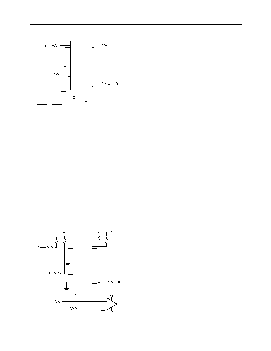
Voltage Multiplier/Divider
Figure 3. Voltage Multiplier/Divider
Extended Range
The input and output voltage ranges can be extended to
include 0 and negative voltage signals by adding bias
currents. The R
S
C
S
filter circuits are eliminated when the
input and biasing resistors are selected to limit the respective
currents to 50 µA min. and 250 µA max.
Extended Range Multiplier
Figure 4. Extended Range Multiplier
65-4200-04
RC4200
V
Z
R
1
V
S
I
3
3
6
4
5
8
7
1
2
I
2
I
1
I
4
V
X
V
Y
R
2
R
4
R
O
V
O
V
X
V
Y
R
1
R
2
=
V
O
V
Z
R
O
R
4
Solving for V
0
V
X
V
Y
R
0
R
4
V
Z
R
1
R
2
--------------------------------------
=
For a multiplier circuit V
Z
V
R
cons
t
tan
=
=
Therefore: V
0
V
X
V
Y
K where K
R
0
R
4
V
R
R
1
R
2
---------------------
=
=
For a divider circuit V
Y
V
R
cons
t
tan
=
=
Therefore: V
0
V
X
V
Z
-------- K where K
V
R
R
0
R
4
R
1
R
2
---------------------
=
=
65-4200-05
RC4200
V
X
(Input)
V
Y
(Input)
+V
REF
R
A
R
B
R
O
R
C
V
S
V
S
+V
S
R
D
R
1
R
2
R
C4
R
CX
I
3
V
O
(Output)
3
6
4
5
8
7
1
2
I
2
I
1
I
4
Resistors R
a
and R
b
extend the range of the V
X
and V
Y
inputs by picking values such that:
Resistor R
C
supplies bias current for I
3
which allows the
output to go negative.
Resistors R
CX
and R
CY
permit equation (6) to balance, ie.:
Cross-Product Cancellation
Cross-products are a result of ths
V
X
V
R
and V
Y
V
R
terms.
To the extend that R
1
R
b
= R
CX
R
D
, and R
2
R
a
= R
CY
R
d
cross-product cancellation will occur.
Arithmetic Offset Cancellation
The offset caused by the V
REF
2
term will cancel to the
extent that R
a
R
b
=
R
0
R
d
, and the result is:
Resistor Values
Inputs:
I
1
min.
(
)
V
X
min.
(
)
R
1
------------------------
V
REF
R
a
--------------
+
50 µA,
=
=
and I
1
(max.)
V
X
(max.)
R
1
------------------------
V
REF
R
a
--------------
+
250 µA,
=
=
also I
2
(min.)
V
Y
(min.)
R
2
-----------------------
V
REF
R
b
--------------
+
50 µA,
=
=
and I
2
(max.)
V
Y
(max.)
R
2
------------------------
V
REF
R
b
--------------
+
250 µA.
=
=
V
X
R
1
--------
V
REF
R
a
----------------
+
VY
R
2
--------
V
REF
R
b
----------------
+
V
0
R
0
-------
V
REF
R
C
----------------
V
X
R
CX
-------------
V
Y
R
CY
-------------
+
+
+
VREF
R
D
----------------
=
V
Y
V
X
R
1
R
2
------------------
V
X
V
REF
R
1
R
b
-------------------------
V
Y
V
REF
R
2
R
a
-------------------------
V
REF
R
a
R
b
---------------- =
+
+
+
V
0
V
REF
R
0
R
d
------------------------
V
X
V
REF
R
cx
R
d
-------------------------
V
Y
V
REF
R
CY
R
d
-------------------------
V
REF
2
R
c
R
d
----------------
+
+
+
V
Y
V
X
R
1
R
2
----------------
V
0
V
REF
R
0
R
d
--------------------- or V
0
V
X
V
Y
K
=
=
where K =
R
0
R
d
V
REF
R
1
R
2
----------------------------
V
X
min.
(
) V
X
V
X
(max.)
V
X
V
X
(max.)
=
V
X
(min.)
V
Y
min.
(
) V
Y
V
Y
(max.)
V
Y
V
Y
(max.) =
=
V
Y
(min.)
V
REF
Constant (+7V to +18V)
=
K
V
0
V
X
V
Y
---------------- Design Requirements
(
)
=