 | ÐлекÑÑоннÑй компоненÑ: RC5532A | СкаÑаÑÑ:  PDF PDF  ZIP ZIP |
Äîêóìåíòàöèÿ è îïèñàíèÿ www.docs.chipfind.ru
www.fairchildsemi.com
REV. 1.1.3 6/14/01
Features
· Small signal bandwidth 10 MHz
· Output drive capability 600
, 10 VRMS
· Input noise voltage 5 nV/
· DC voltage gain 50,000
· AC voltage gain 2200 at 10 KHz
· Power bandwidth 140 KHz
· Slew rate 8 V/µS
· Large supply voltage range ±3V to ±20V
Description
The RC5532 is a high performance, dual low noise opera-
tional amplifier. Compared to standard dual operational
amplifiers, such as the RC747, it shows better noise perfor-
mance, improved output drive capability, and considerably
higher small-signal and power bandwidths.
This makes the device especially suitable for application in
high quality and professional audio equipment, instrumenta-
tion, control circuits, and telephone channel amplifiers.
The op amp is internally compensated for gains equal to one.
If very low noise is of prime importance, it is recommended
that the RC5532A version be used which has guaranteed
noise specifications.
Hz
RC5532/RC5532A
High Performance Dual Low Noise
Operational Amplifier
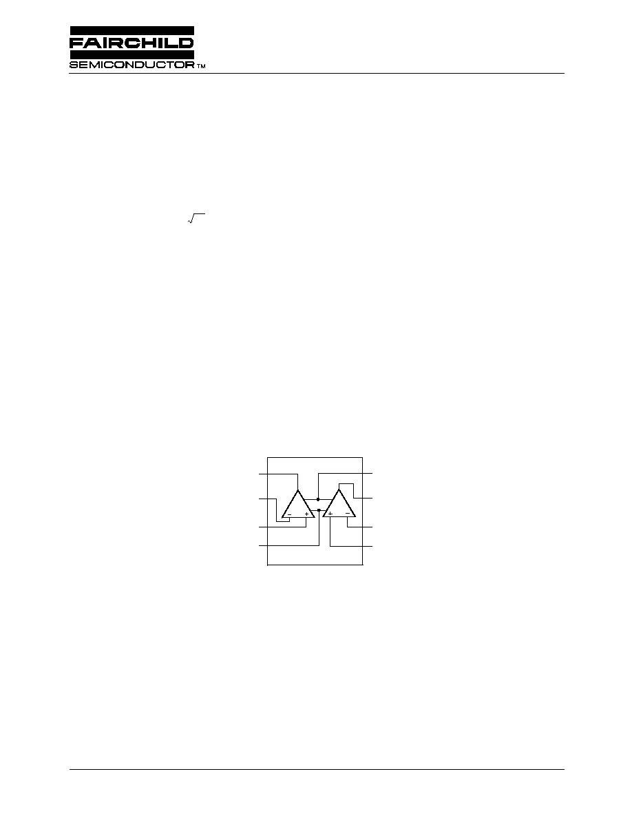
Block Diagram
A
B
65-5532-01
Output A
Input A
+Input A
VS
+VS
Output B
Input B
+Input B
RC5532/RC5532A
PRODUCT SPECIFICATION
2
REV. 1.1.3 6/14/01
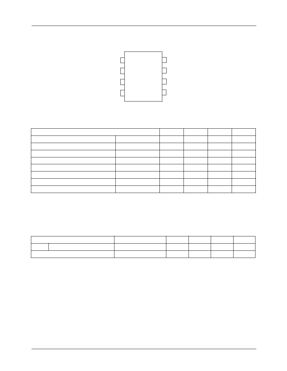
Pin Assignments
Absolute Maximum Ratings
(beyond which the device may be damaged)1
Notes:
1. Functional operation under any of these conditions is NOT implied.
2. For supply voltages less than ±15V, the absolute maximum input voltage is equal to the supply voltage.
3. Short circuit to ground on one amplifier only.
Operating Conditions
Parameter
Min.
Typ.
Max.
Units
Supply Voltage
±22
V
Input Voltage
±V
S
V
Differential Input Voltage
0.5
V
P
D
T
A
< 50°C
PDIP
468
mW
Junction Temperature
PDIP
125
°C
Storage Temperature
-65
150
°C
Operating Temperature
RC5532/A
0
70
°C
Lead Soldering Temperature (10 sec)
300
°C
Parameter
Min.
Typ.
Max.
Units
JA
Thermal resistance
PDIP
160
°C/W
For T
A
> 50°C Derate at
PDIP
6.25
mW/°C
Output (A)
Input (A)
+Input (A)
V
S
+V
S
Output (B)
Input (B)
+Input (B)
1
2
3
4
8
7
6
5
8 PIN PDIP
PRODUCT SPECIFICATION
RC5532/RC5532A
REV. 1.1.3 6/14/01
3
DC Electrical Characteristics
(V
S
= ±15V and T
A
= +25°C unless otherwise noted)
Notes:
1. Diodes protect the inputs against over-voltage. Therefore, unless current-limiting resistors are used, large currents will flow
if the differential input voltage exceeds 0.6V. Maximum input current should be limited to ±10mA.
2. Over Temperature: RC = 0°C
T
A
70°C
Electrical Characteristics
(V
S
= ±15V and T
A
= +25°C )
RC5532/5532A
Parameters
Test Conditions
Min.
Typ.
Max.
Units
Input Offset Voltage
0.5
4.0
mV
Over Temperature
5.0
mV
Input Offset Current
10
150
nA
Over Temperature
200
nA
Input Bias Current
200
800
nA
Over Temperature
1000
nA
Supply Current
6.0
16
mA
Over Temperature
22
mA
Input Voltage Range
±12
±13
V
Common Mode Rejection Ratio
70
100
dB
Power Supply
Rejection Ratio
80
100
dB
Large Signal
Voltage Gain
R
L
2 K
, V
OUT
= ±10V
25
100
V/mV
Over Temperature
15
50
R
L
600
, V
OUT
= ±10V
15
50
Over Temperature
10
Output Voltage Swing
R
L
600
±12
±13
V
R
L
= 600
, V
S
= ±18V
±15
±16
R
L
2k
Input Resistance
(Diff. Mode)
300
K
Short Circuit Current
38
mA
RC/RM5532A
Parameters
Test Conditions
Min.
Typ.
Max.
Units
Input Noise Voltage Density
F
O
= 30 Hz
8.0
12
nV/
Hz
F
O
= 1 kHz
5.0
6.0
Input Noise Current Density
F
O
= 30 Hz
2.7
pA/
Hz
F
O
= 1 kHz
0.7
Channel Separation
F = 1 kHz, R
S
= 5 k
110
dB
RC5532/RC5532A
PRODUCT SPECIFICATION
4
REV. 1.1.3 6/14/01
AC Electrical Characteristics
(V
S
= ±15V and T
A
= +25°C )
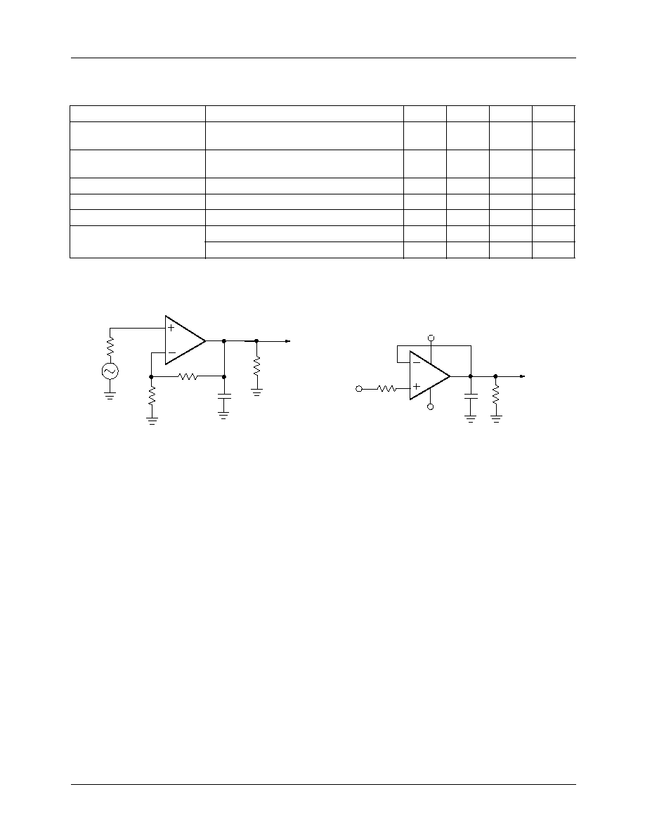
Test Circuits
Figure 1. Closed Loop Frequency Response
Figure 2. Follower, Transient Response
Parameters
Test Conditions
Min.
Typ.
Max.
Units
Output Resistance
A
V
= 30 dB Closed Loop, F = 10 kHz,
R
L
= 600
0.3
Overshoot
Unity Gain, V
IN
= 100 mV
p-p
C
L
= 100 pF, R
L
= 600
10
%
Gain
F = 10 KHz
2.2
V/mV
Gain Bandwidth Product
C
L
= 100 pF, R
L
= 600
10
MHz
Slew Rate
8.0
V/µS
Power Bandwidth
V
OUT
= ±10V
140
KHz
V
OUT
= ±14V, R
L
= 600
, V
S
= ±18V
100
KHz
65-5532-04
R
S
25
5532A
R
F
100 pF
600
3
1
2
V
OUT
V
IN
R
E
65-5532-05
5532A
100 pF
600
V
S
+V
S
V
OUT
1K
V
IN
3
2
1
PRODUCT SPECIFICATION
RC5532/RC5532A
REV. 1.1.3 6/14/01
5
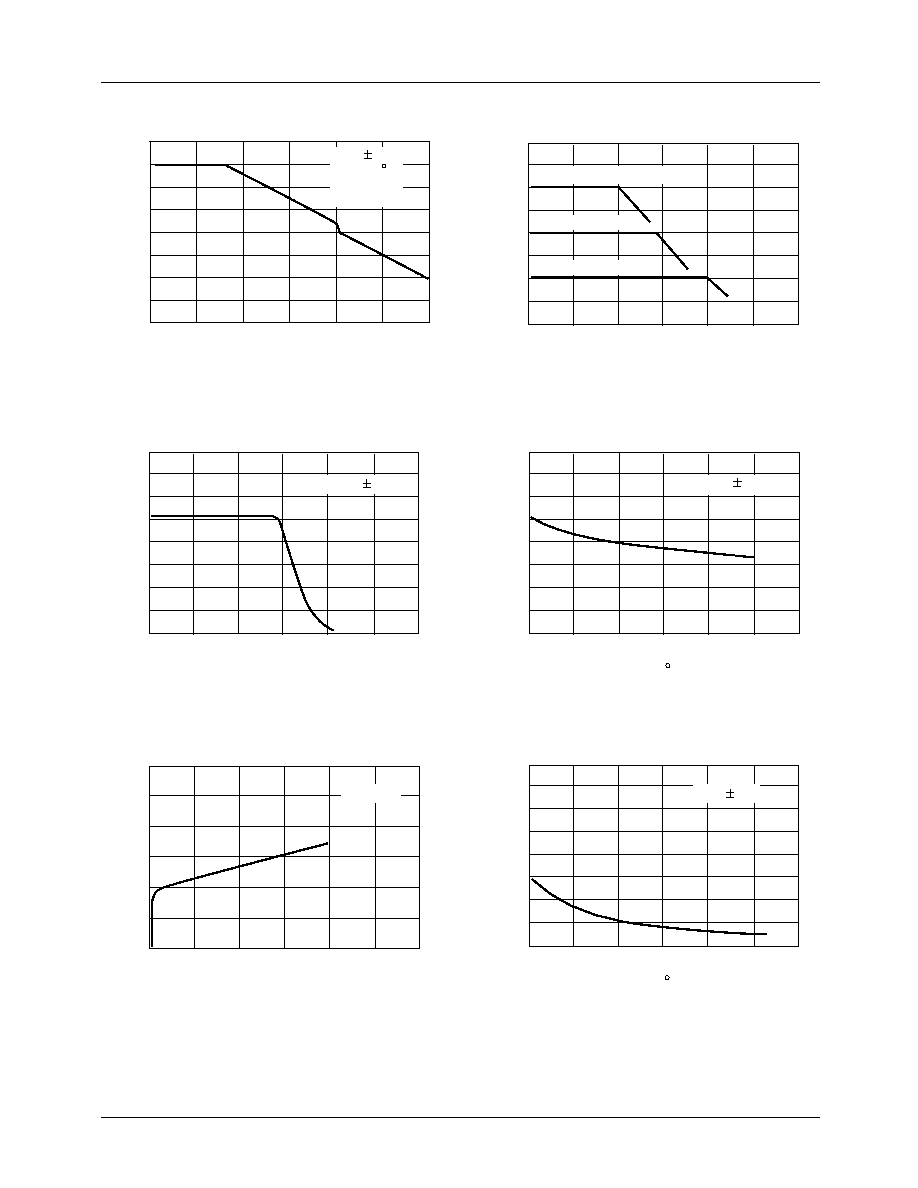
Typical Performance Characteristics
Figure 3. Open Loop Gain vs. Frequency
Figure 4. Closed Loop Gain vs. Frequency
Figure 5. Output Voltage Swing vs. Frequency
Figure 6. Short Circuit Current vs. Temperature
Figure 7. Supply Current vs. Supply Voltage
Figure 8. Input Bias Current vs. Temperature
A
VOL
(dB)
F (Hz)
65-5532-06
120
80
40
0-
40
10
100
1K
10K
1M
10M
V = 15V
T = +25 C
R = 10
A = 40 dB
S
A
S
V
100K
A
VCL
(dB)
F (Hz)
65-5532-07
60
40
20
0
-20
1G
1K
10K
100K
1M
10M
100M
R
F
= 10 K R
E
= 100
R
F
= 9 K R
E
= 1 k
R
F
= 1 K R
E
=
8
V (V)
F (Hz)
65-5532-08
40
30
20
10
0
100M
100
1K
10K
100K
1M
10M
OUT p-P
V = 15V
S
I (mA)
T ( C)
65-5532-09
80
60
40
20
0
A
-55
-25
0
+25
+50
+75
+150
V = 15V
S
SC
I (mA)
+V
S
/-V
S
(V)
65-5532-10
12
8
4
0
0
SY
I = 0
o
UT
±10
±20
±30
I ( A)
T ( C)
65-5532-11
1.4
1.2
0.8
0.4
0
-55
-25
0
+25
+50
+75
+150
µ
B
A
V = 15V
S