6-189
File Number
2837.1
CAUTION: These devices are sensitive to electrostatic discharge; follow proper ESD Handling Procedures.
http://www.intersil.com or 407-727-9207
|
Copyright
©
Intersil Corporation 1999
RFD4N06L, RFD4N06LSM
4A, 60V, 0.600 Ohm, Logic Level,
N-Channel Power MOSFETs
The RFD4N06L, RFD4N06LSM are N-Channel enhancement
mode silicon gate power field effect transistors specifically
designed for use with logic level (5 volt) driving sources in
applications such as programmable controllers, automotive
switching, and solenoid drivers. This performance is
accomplished through a special gate oxide design which
provides full rated conduction at gate biases in the 3-5 volt
range, thereby facilitating true on-off power control from logic
circuit supply voltages.
Formerly developmental type TA09520.
Features
∑ 4A, 60V
∑ r
DS(ON)
= 0.600
∑ Design Optimized for 5 Volt Gate Drive
∑ Can be Driven Directly From Q-MOS, N-MOS,
or TTL Circuits
∑ SOA is Power Dissipation Limited
∑ 175
o
C Rated Junction Temperature
∑ Logic Level Gate
∑ High Input Impedance
∑ Related Literature
- TB334 "Guidelines for Soldering Surface Mount
Components to PC Boards"
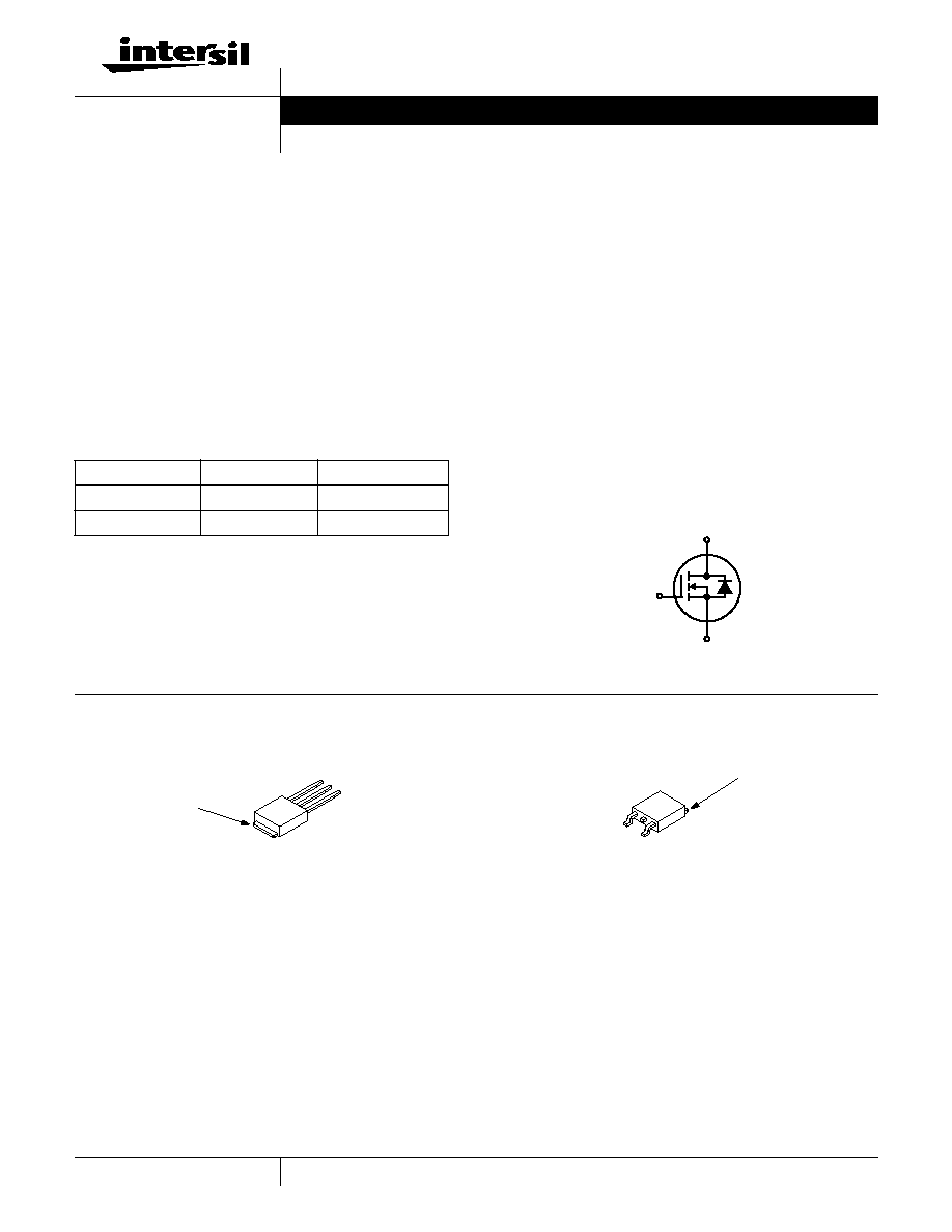
Symbol
Packaging
JEDEC TO-251AA
JEDEC TO-252AA
Ordering Information
PART NUMBER
PACKAGE
BRAND
RFD4N06L
TO-251AA
RFD4N06L
RFD4N06LSM
TO-252AA
RFD4N06LSM
NOTE: When ordering, use the entire part number.
G
D
S
SOURCE
DRAIN
GATE
DRAIN
(FLANGE)
GATE
SOURCE
DRAIN
(FLANGE)
Data Sheet
June 1999

6-190
Absolute Maximum Ratings
T
C
= 25
o
C, Unless Otherwise Specified
RFD4N06L
RFD4N06LSM
UNITS
Drain to Source Breakdown Voltage (Note 1) . . . . . . . . . . . . . . . . . . . . . . . . . . . . . . . . . . . . . . . . V
DS
60
V
Drain to Gate Voltage (Note 1). . . . . . . . . . . . . . . . . . . . . . . . . . . . . . . . . . . . . . . . . . . . . . . . . . .V
DGR
60
V
Gate to Source Voltage . . . . . . . . . . . . . . . . . . . . . . . . . . . . . . . . . . . . . . . . . . . . . . . . . . . . . . . . . V
GS
±1
0
V
Continuous Drain Current . . . . . . . . . . . . . . . . . . . . . . . . . . . . . . . . . . . . . . . . . . . . . . . . . . . . . . . . . I
D
4
A
Pulsed Drain Current (Note 3) . . . . . . . . . . . . . . . . . . . . . . . . . . . . . . . . . . . . . . . . . . . . . . . . . . . . I
DM
10
A
Maximum Power Dissipation . . . . . . . . . . . . . . . . . . . . . . . . . . . . . . . . . . . . . . . . . . . . . . . . . . . . . . P
D
Derated above 25
o
C. . . . . . . . . . . . . . . . . . . . . . . . . . . . . . . . . . . . . . . . . . . . . . . . . . . . . . . . . . . . .
30
0.20
W
W/
o
C
Operating and Storage Temperature . . . . . . . . . . . . . . . . . . . . . . . . . . . . . . . . . . . . . . . . . . . T
J,
T
STG
-55 to 175
o
C
Maximum Temperature for Soldering
Leads at 0.063in (1.6mm) from Case for 10s . . . . . . . . . . . . . . . . . . . . . . . . . . . . . . . . . . . . . . . . T
L
Package Body for 10s, See Techbrief 334 . . . . . . . . . . . . . . . . . . . . . . . . . . . . . . . . . . . . . . . . . T
pkg
300
260
o
C
o
C
CAUTION: Stresses above those listed in "Absolute Maximum Ratings" may cause permanent damage to the device. This is a stress only rating and operation of the
device at these or any other conditions above those indicated in the operational sections of this specification is not implied.
NOTE:
1. T
J
= 25
o
C to 150
o
C.
Electrical Specifications
T
C
= 25
o
C, Unless Otherwise Specified
PARAMETER
SYMBOL
TEST CONDITIONS
MIN
TYP
MAX
UNITS
Drain to Source Breakdown Voltage
BV
DSS
I
D
= 1mA, V
GS
= 0V
60
-
-
V
Gate to Threshold Voltage
V
GS(TH)
V
GS
= V
DS
, I
D
= 250
µ
A
1
-
2.5
V
Zero Gate Voltage Drain Current
I
DSS
T
C
= 25
o
C, V
DS
= 50V, V
GS
= 0V
-
-
1
µ
A
T
C
= 125
o
C, V
DS
= 50V, V
GS
= 0V
-
-
50
µ
A
Gate to Source Leakage Current
I
GSS
V
GS
= 10V, V
DS
= 0V
-
-
100
nA
Drain to Source On Voltage (Note 2)
V
DS(ON)
I
D
= 1A, V
GS
= 5V
-
-
0.8
V
I
D
= 2A, V
GS
= 5V
-
-
2.0
V
I
D
= 4A, V
GS
= 7.5V
-
-
4.0
V
Drain to Source On Resistance (Note 2)
r
DS(ON)
I
D
= 1A, V
GS
= 5V
-
-
0.600
Forward Transconductance (Note 2)
V(plateau) V
DS
= 15V, I
D
= 4A
-
-
4.5
V
Turn-On Delay Time
t
d(ON)
V
DD
= 30V, I
D
= 1A, R
GS
= 6.25
,
V
GS
= 5V
-
-
20
ns
Rise Time
t
r
-
-
130
ns
Turn-Off Delay Time
t
d(OFF)
-
-
40
ns
Fall Time
t
f
-
-
160
ns
Total Gate Charge
(Gate to Source + Gate to Drain)
Q
g(TOT)
V
GS
= 0-10V
V
DD
= 48V,
I
D
= 2A,
R
L
= 24
-
-
8
nC
Gate Charge at 5V
Q
g(5)
V
GS
= 0-5V
-
-
5
nC
Threshold Gate Charge
Q
g(TH)
V
GS
= 0-1V
-
-
1
nC
Thermal Resistance Junction to Case
R
JC
-
-
5
o
C/W
Source to Drain Diode Specifications
PARAMETER
SYMBOL
TEST CONDITIONS
MIN
TYP
MAX
UNITS
Source to Drain Diode Voltage (Note 2)
V
SD
I
SD
= 1A
-
-
1.4
V
Reverse Recovery Time
t
rr
I
SD
= 2A, dI
SD
/dt = 100A/
µ
s
-
150
-
ns
NOTES:
2. Pulsed: pulse duration = 300
µ
s max, duty cycle = 2%.
3. Repetitive rating: pulse width limited by maximum junction temperature.
RFD4N06L, RFD4N06LSM

6-191
Typical Performance Curves
Unless Otherwise Specified
FIGURE 1. NORMALIZED POWER DISSIPATION vs CASE
TEMPERATURE
FIGURE 2. MAXIMUM CONTINUOUS DRAIN CURRENT vs
CASE TEMPERATURE
FIGURE 3. FORWARD BIAS SAFE OPERATING AREA
FIGURE 4. SATURATION CHARACTERISTICS
FIGURE 5. TRANSFER CHARACTERISTICS
FIGURE 6. DRAIN TO SOURCE ON RESISTANCE vs DRAIN
CURRENT
T
C
, CASE TEMPERATURE (
o
C)
0
25
50
75
100
125
150
1.2
1.0
0.8
0.6
0.4
0.2
0
PO
WER DISSIP
A
TION MUL
TIPLIER
0
25
50
75
100
125
150
T
C
, CASE TEMPERATURE (
o
C)
I
D
, DRAIN CURRENT (A)
5
3
2
1
4
V
DS
, DRAIN TO SOURCE VOLTAGE (V)
10
0.1
10
1
I
D
, DRAIN CURRENT (A)
100
1.0
T
J
= MAX RATED
T
C
= 25
o
C
OPERATION IN THIS AREA
LIMITED BY r
DS(ON)
12
10
8
6
4
2
0
0
1
2
3
4
5
6
7
I
D
, DRAIN CURRENT (A)
V
DS
, DRAIN TO SOURCE VOLTAGE (V)
PULSE DURATION = 80
µ
s
T
C
= 25
o
C
V
GS
= 7.5V
V
GS
= 10V
V
GS
= 5V
4.5V
4V
3.5V
3V
2.5V
2V
V
GS
, GATE TO SOURCE VOLTAGE (V)
I
DS(ON)
, DRAIN T
O
SOURCE CURRENT (A)
T
C
= -40
o
C
T
C
= -40
o
C
T
C
= 125
o
C
5
4
3
2
1
0
1
2
3
4
5
6
8
7
6
V
DS
= 10V
PULSE DURATION = 80
µ
s
DUTY CYCLE
2%
T
C
= 25
o
C
T
C
= 125
o
C
I
D
, DRAIN CURRENT (A)
r
DS(ON)
, DRAIN T
O
SOURCE
ON RESIST
ANCE(
)
T
C
= 25
o
C
T
C
= -40
o
C
1.4
1.2
1.0
0.8
0.6
0.4
0.2
0
1.6
0
2
4
6
8
10
V
GS
= 5V
PULSE DURATION = 80
µ
s
T
C
= 125
o
C
RFD4N06L, RFD4N06LSM
6-192
FIGURE 7. NORMALIZED DRAIN TO SOURCE ON
RESISTANCE vs JUNCTION TEMPERATURE
FIGURE 8. NORMALIZED GATE THRESHOLD VOLTAGE vs
JUNCTION TEMPERATURE
FIGURE 9. CAPACITANCE vs DRAIN TO SOURCE VOLTAGE
NOTE: Refer to Intersil Application Notes AN7254 and AN7260.
FIGURE 10. NORMALIZED SWITCHING WAVEFORMS FOR
CONSTANT GATE CURRENT
Test Circuits and Waveforms
FIGURE 11. SWITCHING TIME TEST CIRCUIT
FIGURE 12. RESISTIVE SWITCHING WAVEFORMS
Typical Performance Curves
Unless Otherwise Specified (Continued)
0
-50
0
50
100
150
200
T
J
, JUNCTION TEMPERATURE (
o
C)
2
1.5
1
0.5
NORMALIZED DRAIN T
O
SOURCE ON RESIST
ANCE
V
GS
= 5V, I
D
= 2A
0
-50
0
50
100
150
200
T
J
, JUNCTION TEMPERATURE (
o
C)
2
1.5
1
0.5
NORMALIZED GA
TE
THRESHOLD V
O
L
T
A
GE
V
GS
= V
DS
, I
D
= 250
µ
A
0
10
20
30
40
50
300
400
0
100
200
V
DS
, DRAIN TO SOURCE VOLTAGE (V)
C, CAP
A
CIT
ANCE (pF)
C
ISS
C
OSS
C
RSS
V
GS
= 0V, f = 1MHz
C
ISS
= C
GS
+ C
GD
C
RSS
= C
GD
C
OSS
C
DS
+ C
GD
60
45
30
15
0
10
8
6
4
2
0
GATE SOURCE
VOLTAGE
R
L
= 4
I
G(REF)
= 0.5mA
V
GS
= 5V
DRAIN SOURCE VOLTAGE
0.75BV
DSS
0.50BV
DSS
0.25BV
DSS
V
DS
, DRAIN T
O
SOURCE V
O
L
T
A
GE (V)
V
GS
, GA
TE T
O
SOURCE V
O
L
T
A
GE (V)
I
G(REF)
I
G(ACT)
20
I
G(REF)
I
G(ACT)
80
t, TIME (
µ
s)
V
DD
= BV
DSS
V
DD
= BV
DSS
V
GS
R
L
R
G
DUT
+
-
V
DD
t
ON
t
d(ON)
t
r
90%
10%
V
DS
90%
10%
t
f
t
d(OFF)
t
OFF
90%
50%
50%
10%
PULSE WIDTH
V
GS
0
0
RFD4N06L, RFD4N06LSM

6-193
All Intersil semiconductor products are manufactured, assembled and tested under ISO9000 quality systems certification.
Intersil semiconductor products are sold by description only. Intersil Corporation reserves the right to make changes in circuit design and/or specifications at any time with-
out notice. Accordingly, the reader is cautioned to verify that data sheets are current before placing orders. Information furnished by Intersil is believed to be accurate and
reliable. However, no responsibility is assumed by Intersil or its subsidiaries for its use; nor for any infringements of patents or other rights of third parties which may result
from its use. No license is granted by implication or otherwise under any patent or patent rights of Intersil or its subsidiaries.
For information regarding Intersil Corporation and its products, see web site http://www.intersil.com
Sales Office Headquarters
NORTH AMERICA
Intersil Corporation
P. O. Box 883, Mail Stop 53-204
Melbourne, FL 32902
TEL: (407) 724-7000
FAX: (407) 724-7240
EUROPE
Intersil SA
Mercure Center
100, Rue de la Fusee
1130 Brussels, Belgium
TEL: (32) 2.724.2111
FAX: (32) 2.724.22.05
ASIA
Intersil (Taiwan) Ltd.
7F-6, No. 101 Fu Hsing North Road
Taipei, Taiwan
Republic of China
TEL: (886) 2 2716 9310
FAX: (886) 2 2715 3029
RFD4N06L, RFD4N06LSM