 | ÐлекÑÑоннÑй компоненÑ: RFG40N10 | СкаÑаÑÑ:  PDF PDF  ZIP ZIP |
Äîêóìåíòàöèÿ è îïèñàíèÿ www.docs.chipfind.ru
©2002 Fairchild Semiconductor Corporation
RFG40N10, RFP40N10, RF1S40N10, RF1S40N10SM Rev. C
RFG40N10, RFP40N10, RF1S40N10,
RF1S40N10SM
40A, 100V, 0.040 Ohm, N-Channel Power
MOSFETs
These are N-Channel power MOSFETs manufactured using
the MegaFET process. This process, which uses feature
sizes approaching those of LSI integrated circuits gives
optimum utilization of silicon, resulting in outstanding
performance. They were designed for use in applications
such as switching regulators, switching converters, motor
drivers, relay drivers and emitter switches for bipolar
transistors. These transistors can be operated directly from
integrated circuits.
Formerly developmental type TA9846
Features
· 40A, 100V
· r
DS(ON)
= 0.040
· UIS Rating Curve
· SOA is Power Dissipation Limited
· 175
o
C Operating Temperature
· Related Literature
- TB334 "Guidelines for Soldering Surface Mount
Components to PC Boards"
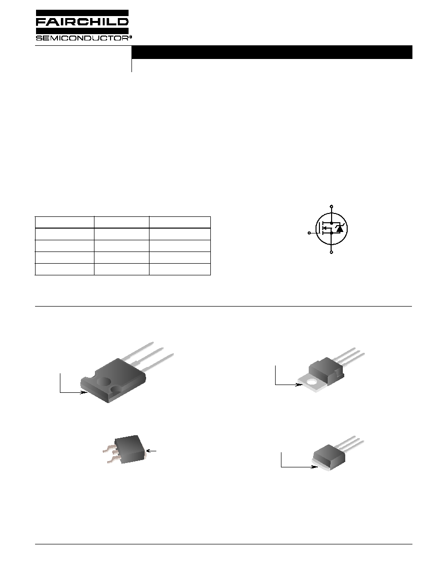
Symbol
Packaging
Ordering Information
PART NUMBER
PACKAGE
BRAND
RFG40N10
TO-247
RFG40N10
RFP40N10
TO-220AB
RFP40N10
RF1S40N10
TO-262AA
F1S40N10
RF1S40N10SM
TO-263AB
F1S40N10
NOTE: When ordering, use the entire part number. Add the suffix, 9A,
to obtain the TO-263AB variant in tape and reel, i.e. RF1S40N10SM9A.
D
G
S
JEDEC STYLE TO-247
JEDEC TO-220AB
JEDEC TO-263AB
JEDEC TO-262AA
DRAIN
(FLANGE)
SOURCE
DRAIN
GATE
DRAIN
(FLANGE)
SOURCE
DRAIN
GATE
DRAIN
(FLANGE)
GATE
SOURCE
DRAIN
SOURCE
GATE
DRAIN
(FLANGE)
Data Sheet
January 2002
©2002 Fairchild Semiconductor Corporation
RFG40N10, RFP40N10, RF1S40N10, RF1S40N10SM Rev. C
Absolute Maximum Ratings
T
C
= 25
o
C, Unless Otherwise Specified
RFG40N10, RFP40N10,
RF1S40N10, RF1S40N10SM
UNITS
Drain to Source Breakdown Voltage (Note 1) . . . . . . . . . . . . . . . . . . . . . . . . . . . V
DSS
100
V
Drain to Gate Voltage (R
GS
= 1M
)
(Note 1) . . . . . . . . . . . . . . . . . . . . . . . . . . V
DGR
100
V
Gate to Source Voltage . . . . . . . . . . . . . . . . . . . . . . . . . . . . . . . . . . . . . . . . . . . . . V
GS
±
20
V
Drain Current
Continuous (Figure 2). . . . . . . . . . . . . . . . . . . . . . . . . . . . . . . . . . . . . . . . . . . . . . .I
D
Pulsed Drain Current (Note 2) . . . . . . . . . . . . . . . . . . . . . . . . . . . . . . . . . . . . . . I
DM
40
100
A
A
Pulsed Avalanche Rating . . . . . . . . . . . . . . . . . . . . . . . . . . . . . . . . . . . . . . . . . . . . E
AS
Figures 4, 12, 13
Power Dissipation . . . . . . . . . . . . . . . . . . . . . . . . . . . . . . . . . . . . . . . . . . . . . . . . . . P
D
Derate Above 25
o
C . . . . . . . . . . . . . . . . . . . . . . . . . . . . . . . . . . . . . . . . . . . . . . . . .
160
1.07
W
W/
o
C
Operating and Storage Temperature . . . . . . . . . . . . . . . . . . . . . . . . . . . . . . . T
J
, T
STG
-55 to 175
o
C
Maximum Temperature for Soldering
Leads at 0.063in (1.6mm) from case for 10s . . . . . . . . . . . . . . . . . . . . . . . . . . . . T
L
Package Body for 10s, see Techbrief 334 . . . . . . . . . . . . . . . . . . . . . . . . . . . . .T
pkg
300
260
o
C
o
C
CAUTION: Stresses above those listed in "Absolute Maximum Ratings" may cause permanent damage to the device. This is a stress only rating and operation of the
device at these or any other conditions above those indicated in the operational sections of this specification is not implied.
NOTES:
1. T
J
= 25
o
C to 150
o
C.
2. Repetitive Rating: pulse width limited by maximum junction temperature.
Electrical Specifications
T
C
= 25
o
C, Unless Otherwise Specified
PARAMETER
SYMBOL
TEST CONDITIONS
MIN
TYP
MAX
UNITS
Drain to Source Breakdown Voltage
BV
DSS
I
D
= 250
µ
A, V
GS
= 0V (Figure 9)
100
-
-
V
Gate Threshold Voltage
V
GS(TH)
V
GS
= V
DS
, I
D
= 250
µ
A (Figure 8)
2
-
4
V
Zero Gate Voltage Drain Current
I
DSS
V
DS
= 80V,
V
GS
= 0V
T
C
= 25
o
C
-
-
1
µ
A
T
C
= 150
o
C
-
-
50
µ
A
Gate to Source Leakage Current
I
GSS
V
GS
=
±
20V
-
-
±
100
nA
Drain to Source On Resistance
r
DS(ON)
I
D
= 40A, V
GS
= 10V (Figure 7)
-
-
0.040
Turn-On Time
t
ON
V
DD
= 50V, I
D
= 20A,
R
L
= 2.5
, V
GS
= 10V, R
GS
= 4.2
(Figure 11)
-
-
80
ns
Turn-On Delay Time
t
d(ON)
-
17
-
ns
Rise Time
t
r
-
30
-
ns
Turn-Off Delay Time
t
d(OFF)
-
42
-
ns
Fall Time
t
f
-
20
-
ns
Turn-Off Time
t
OFF
-
-
100
ns
Total Gate Charge
Q
g(TOT)
V
GS
= 0V to 20V
V
DD
= 80V,
I
D
= 40A,
R
L
= 2.0
(Figures 11)
-
-
300
nC
Gate Charge at 10V
Q
g(10)
V
GS
= 0V to 10V
-
-
150
nC
Threshold Gate Charge
Q
g(TH)
V
GS
= 0V to 2V
-
-
7.5
nC
Thermal Resistance Junction to Case
R
JC
-
-
0.94
o
C/W
Thermal Resistance Junction to Ambient
R
JA
TO-247
-
-
30
o
C/W
TO-220AB and TO-263AB
-
-
62
o
C/W
Source to Drain Diode Specifications
PARAMETER
SYMBOL
TEST CONDITIONS
MIN
TYP
MAX
UNITS
Source to Drain Diode Voltage
V
SD
I
SD
= 40A
-
-
1.5
V
Reverse Recovery Time
t
rr
I
SD
= 40A, dI
SD
/dt = 100A/
µ
s
-
-
200
ns
RFG40N10, RFP40N10, RF1S40N10, RF1S40N10SM
©2002 Fairchild Semiconductor Corporation
RFG40N10, RFP40N10, RF1S40N10, RF1S40N10SM Rev. C
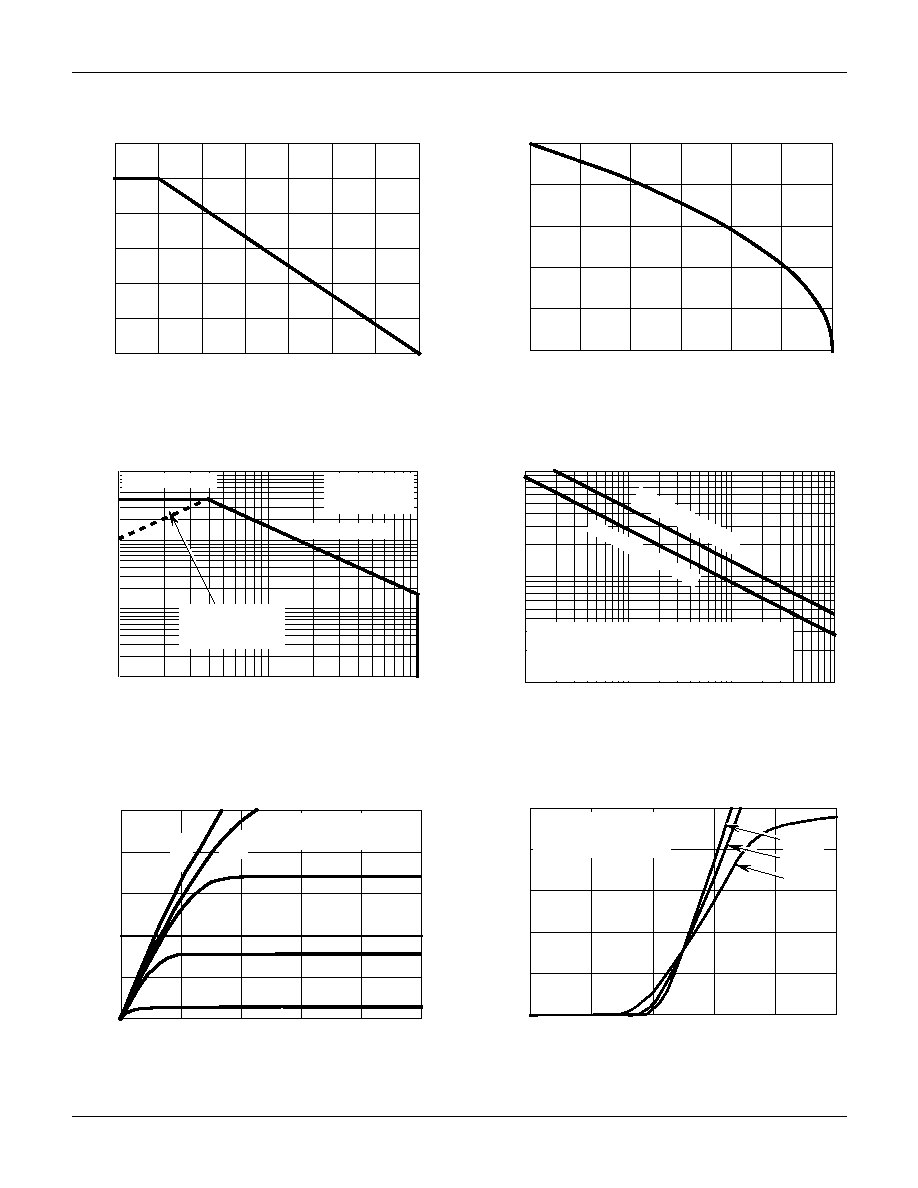
Typical Performance Curves
Unless Otherwise Specified
FIGURE 1. NORMALIZED POWER DISSIPATION vs CASE
TEMPERATURE
FIGURE 2. MAXIMUM CONTINUOUS DRAIN CURRENT vs
CASE TEMPERATURE
FIGURE 3. FORWARD BIAS SAFE OPERATING AREA
NOTE: Refer to application notes AN9321 and AN9322.
FIGURE 4. UNCLAMPED INDUCTIVE SWITCHING
CAPABILITY
FIGURE 5. SATURATION CHARACTERISTICS
FIGURE 6. TRANSFER CHARACTERISTICS
T
C
, CASE TEMPERATURE (
o
C)
PO
WER DISSIP
A
TION MUL
TIPLIER
0
0
25
50
75
100
175
0.2
0.4
0.6
0.8
1.0
1.2
125
150
16
8
0
25
50
75
100
125
150
24
40
32
I
D
,
DRAIN CURRENT (A)
T
C
, CASE TEMPERATURE (
o
C)
175
100
10
1
0.1
1
10
100
V
DS
,
DRAIN TO SOURCE VOLTAGE (V)
OPERATION IN THIS
AREA MAY BE
LIMITED BY r
DS(ON)
V
DSS(MAX)
= 100V
I
D
,
DRAIN CURRENT (A)
T
C
= 25
o
C
DC OPERATION
SINGLE PULSE
T
J
= MAX RATED
t
AV
= (L)(I
AS
)/(1.3 RATED BV
DSS
- V
DD
)
If R = 0
If R
0
t
AV
= (L/R)LN[(I
AS
*R)/(1.3 RATED BV
DSS
- V
DD
) + 1]
ST
AR
TING T
J
= 25
o
C
ST
AR
TING
T
J
= 150
o
C
t
AV
, TIME IN AVALANCHE (ms)
I
AS
,
A
V
ALANCHE CURRENT (A)
0.1
1
10
0.01
10
100
1
100
80
60
40
20
0
0
2
4
6
8
10
I
D
,
DRAIN CURRENT (A)
V
DS,
DRAIN TO SOURCE VOLTAGE (V)
V
GS
= 10V
V
GS
= 7V
V
GS
= 6V
V
GS
= 5V
V
GS
= 4V
T
C
= 25
o
C
PULSE DURATION = 80
µs
DUTY CYCLE = 0.5% MAX
0
2
4
6
8
10
V
GS
,
GATE TO SOURCE VOLTAGE (V)
I
D,
DRAIN CURRENT (A)
100
80
60
40
20
0
PULSE DURATION = 80
µs
DUTY CYCLE = 0.5% MAX
V
DD
= 15V
-55
o
C
25
o
C
175
o
C
RFG40N10, RFP40N10, RF1S40N10, RF1S40N10SM
©2002 Fairchild Semiconductor Corporation
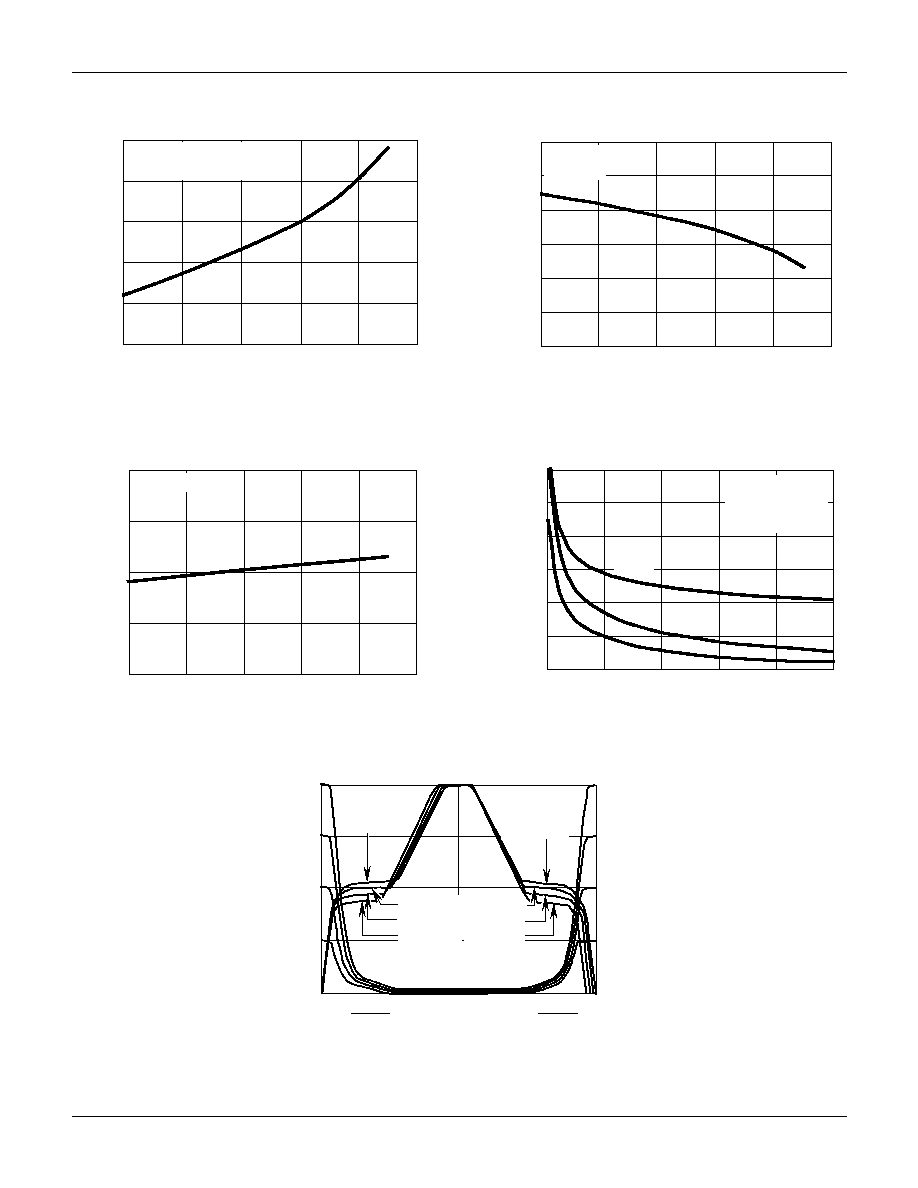
RFG40N10, RFP40N10, RF1S40N10, RF1S40N10SM Rev. C
FIGURE 7. NORMALIZED DRAIN TO SOURCE ON
RESISTANCE vs JUNCTION TEMPERATURE
FIGURE 8. NORMALIZED GATE THRESHOLD VOLTAGE vs
JUNCTION TEMPERATURE
FIGURE 9. NORMALIZED DRAIN TO SOURCE BREAKDOWN
VOLTAGE vs JUNCTION TEMPERATURE
FIGURE 10. CAPACITANCE vs DRAIN TO SOURCE VOLTAGE
NOTE: Refer to Application Notes AN7254 and AN7260.
FIGURE 11. NORMALIZED SWITCHING WAVEFORMS FOR CONSTANT GATE CURRENT
Typical Performance Curves
Unless Otherwise Specified (Continued)
2.5
2.0
1.5
1.0
0.5
0
-50
0
50
100
150
200
NORMALIZED DRAIN
T
O
SOURCE
T
J,
JUNCTION TEMPERATURE (
o
C)
PULSE DURATION = 80
µs
V
GS
= 10V, I
D
= 40A
ON RESIST
ANCE
DUTY CYCLE = 0.5% MAX
1.50
1.25
1.00
0.75
0
-50
0
50
100
150
200
THRESHOLD V
O
L
T
A
G
E
T
J,
JUNCTION TEMPERATURE (
o
C)
NORMALIZED GA
TE
0.50
0.25
V
GS
= V
DS
I
D
= 250
µA
2.0
1.5
1.0
0.5
0
-50
0
50
100
150
200
NORMALIZED DRAIN
T
O
SOURCE
BREAKDO
WN V
O
L
T
A
G
E
T
J,
JUNCTION TEMPERATURE (
o
C)
I
D
= 250
µA
C
ISS
C
OSS
C
RSS
6000
4000
2000
1000
0
0
5
10
15
20
25
C
,
CAP
A
CIT
ANCE (pF)
V
DS
, DRAIN TO SOURCE VOLTAGE (V)
5000
3000
V
GS
= 0V, f = 1MHz
C
ISS
= C
GS
+ C
GD
C
RSS
= C
GD
C
OSS
C
DS
+ C
GD
100
75
50
25
0
10
7.5
5.0
2.5
0
V
GS
,
GA
TE
T
O
SOURCE
V
O
L
T
A
GE (V)
20
I
g(REF)
I
g(ACT)
80
I
g(REF)
I
g(ACT)
t, TIME (
µs)
R
L
= 2.5
I
g(REF)
= 2.25mA
V
GS
= 10V
V
DS
,
DRAIN
T
O
SOURCE
V
O
L
T
A
GE (V)
V
DD
= BV
DSS
V
DD
= BV
DSS
0.75 BV
DSS
0.50 BV
DSS
0.25 BV
DSS
0.50 BV
DSS
0.25 BV
DSS
0.75 BV
DSS
RFG40N10, RFP40N10, RF1S40N10, RF1S40N10SM
©2002 Fairchild Semiconductor Corporation
RFG40N10, RFP40N10, RF1S40N10, RF1S40N10SM Rev. C
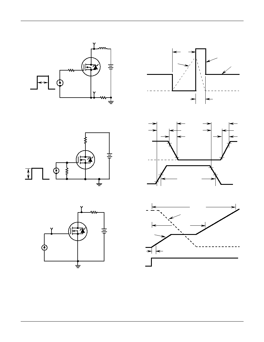
Test Circuits and Waveforms
FIGURE 12. UNCLAMPED ENERGY TEST CIRCUIT
FIGURE 13. UNCLAMPED ENERGY WAVEFORMS
FIGURE 14. SWITCHING TIME TEST CIRCUIT
FIGURE 15. RESISTIVE SWITCHING WAVEFORMS
FIGURE 16. GATE CHARGE TEST CIRCUIT
FIGURE 17. GATE CHARGE WAVEFORMS
t
P
V
GS
0.01
L
I
AS
+
-
V
DS
V
DD
R
G
DUT
VARY t
P
TO OBTAIN
REQUIRED PEAK I
AS
0V
V
DD
V
DS
BV
DSS
t
P
I
AS
t
AV
0
V
GS
R
L
R
GS
DUT
+
-
V
DD
t
ON
t
d(ON)
t
r
90%
10%
V
DS
90%
10%
t
f
t
d(OFF)
t
OFF
90%
50%
50%
10%
PULSE WIDTH
V
GS
0
0
R
L
V
GS
+
-
V
DS
V
DD
DUT
I
g(REF)
V
DD
Q
g(TH)
V
GS
= 2V
Q
g(10)
V
GS
= 10V
Q
g(TOT)
V
GS
= 20V
V
DS
V
GS
I
g(REF)
0
0
RFG40N10, RFP40N10, RF1S40N10, RF1S40N10SM