Äîêóìåíòàöèÿ è îïèñàíèÿ www.docs.chipfind.ru
©2004 Fairchild Semiconductor Corporation
May 2004
RMBA19500A Rev. C
RMBA19500A
RMBA19500A
PCS1900 2 Watt GaAs MMIC Power Amplifier
General Description
The RMBA19500A is a highly linear Power Amplifier. The
two stage circuit uses our pHEMT process. It has been
designed for use as a driver stage for PCS1900 base
stations, or as the output stage for Micro- and Pico-Cell
base stations. The amplifier has been optimized for high
linearity requirements for PCS operation.
Features
· 2 Watt linear output power at 36 dBc ACPR1 for CDMA
operation
· OIP3
43 dBm at 27 and 30 dBm output
· Small Signal Gain of > 30 dB
· Small outline SMD package
Absolute Ratings
Electrical Characteristics
2
Notes:
1. Only under quienscent conditions--no RF applied.
2. V
DD
= 7.0V, T
C
= 25°C. Part mounted on evaluation board with input and output matching to 50
.
3. 9 Channel Forward Link QPSK Source; 1.23 Mbps modulation rate. CDMA ACPR1 is measured using the ratio of the average power within the 1.23 MHz channel
at band center to the average power within a 30 KHz bandwidth at an 885 KHz offset. Minimum CDMA output power is met with ACPR1 > 36 dBc.
4. OIP3 specifications are achieved for power output levels of 27 and 30 dBm per tone with tone spacing of 1.25 MHz at band-center with adjusted supply and bias
conditions of Vdd = 6.5V and IdqTotal = 625mA (see Note 5).
5. VG1,2 and VG3 must be individually adjusted to achieve IDQ1,2 and IDQ3. A single VGG bias supply adjusted to achieve IDQTOTAL = 625mA can be used with
nearly equivalent performance. Values for IDQ1,2 and IDQ3 shown have been optimized for CDMA operation. IDQ1, 2 and IDQ3 (or IDQTOTAL) can be adjusted
to optimize the linearity of the amplifier for other modulation systems.
The device requires external input and output matching to 50
as shown in Figure 3 and the Parts List.
Symbol
Parameter
Ratings
Units
Vd
Drain Supply Voltage
1
+10
V
Vg
Gate Supply Voltage (max absolute)
-5
V
P
IN
RF Input Power (from 50
source)
+5
dBm
T
C
Operating Case Temperature Range
-30 to +85
°C
T
STG
Storage Temperature Range
-40 to +100
°C
Parameter
Min
Typ
Max
Units
Frequency Range
1930
1990
MHz
Gain (Small Signal) Over 19301990 MHz
30
dB
Gain Variation
Over Frequency Range
Over Temperature Range
±1.0
±1.5
dB
dB
Noise Figure
6
dB
P1dB Output
30
dBm
Output Power @ CDMA
3
33
dBm
PAE @ 33 dBm Pout
24
%
OIP3
4
43
45
dBm
Drain Voltage (Vdd)
7.0
V
Gate Voltage (VG1, 2 and VG3)
5
-2
-0.25
V
Quiescent currents (Idq1, 2 and Idq3)
5
180, 445
mA
Thermal Resistance (Channel to Case) R
JC
11
°C/W
©2004 Fairchild Semiconductor Corporation
RMBA19500A Rev. C
RMBA19500A
Application Information
CAUTION: THIS IS AN ESD SENSITIVE DEVICE
The following describes a procedure for evaluating the RMBA19500A, a monolithic high efficiency power amplifier, in a
surface mount package, designed for use as a driver stage for PCS1900 Base station or as the final output stage for Micro-
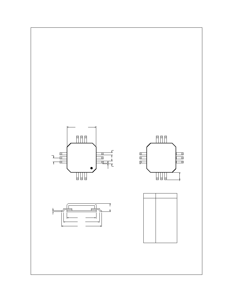
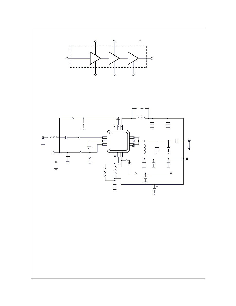
and Pico-Cell base stations. Figure 1 shows the package outline and the pin designations. Figure 2 shows the functional
block diagram of the packaged product. The RMBA19500A requires external passive components for DC bias and RF input
and output matching circuits as shown in Figure 3 and the Parts List. A recommended schematic circuit is shown in Figure
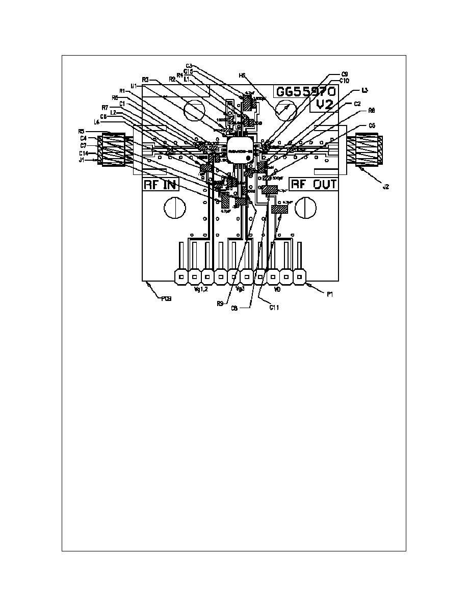
3. The gate biases for the three stages of the amplifier may be set by simple resistive voltage dividers. Figure 4 shows a
typical layout of an evaluation board, corresponding to the schematic circuits of Figure 3. The following designations should
be noted:
(1) Pin designations are as shown in Figure 2.
(2) Vg1, Vg2, and Vg3 are the Gate Voltages (negative) applied at the pins of the package.
(3) Vgg1, 2, and Vgg3 are the negative supply voltages at the evaluation board terminals (Vg1 and Vg2 are tied together).
(4) Vd1, Vd2, and Vd3 are the Drain Voltages (positive) applied at the pins of the package.
(5) Vdd is the positive supply voltage at the evaluation board terminal (Vd1, Vd2, and Vd3 are tied together).
Note: The base of the package must be soldered on to a heat sink for proper operation.
Figure 1. Package Outline and Pin Designations
6
5
0.200 SQ.
0.011
RMBA19500A
0.030
0.020
0.015
4
4
5
Bottom View
Top View
Plastic Lid
Side Section
6
12 11 10
7
8
9
3
2
1
10
3
2
1
7
8
9
11 12
0.041
0.075 MAX
0.010
Dimensions in inches
0.282
0.246
0.230
Pin Description
1
RF Out & Vd3
2
RF Out & Vd3
3
RF Out & Vd3
4 VD1
5 GND
6 VG1
7 RF
In
8 GND
9 VG2
10 VD2
11 GND
12 VG3
13 GND
©2004 Fairchild Semiconductor Corporation
RMBA19500A Rev. C
RMBA19500A
Figure 2. Functional Block Diagram
Figure 3. Schematic of Application Circuit Showing External Components
MMIC CHIP
Vg1
Pin #6
Vg 2
Pin # 9
Vd1
Pin #4
Vd2
Pin #10
GND
Pin #5, 8, 11, 13
Vg 3
Pin #12
RF IN
Pin #7
RF OUT & Vd3
Pin #1, 2, 3
Fairchild
RMBA19500A
R2
1k
R3
910
R1
20
C1
10pF
C6
0.1
µF
C7
0.1
µF
C8
4.7
µF
C9
2.2pF
C10
2.2pF
C5
1500pF
C3
1500pF
C2
10.0pF
J2
RFOUT
R5
20
R4
30
C4
1500pF
L2
5.6nH
P2
P4
VD1, 2, 3
VGG3
P3
GND
P1
VG1, VG2
J1
RFIN
C14
4.7
µF
C11
4.7
µF
R8
390
R9
300
R7
1K
R6
1.1K
C15
4.7µF
L3
10nH
L1
5.6nH
L4
5.6nH
©2004 Fairchild Semiconductor Corporation
RMBA19500A Rev. C
RMBA19500A
Figure 4. Layout of Test Evaluation Board (RMBA19500A-TB, G655971)
Test Procedure for the Evaluation Board (RMBA19500A-TB)
CAUTION: LOSS OF GATE VOLTAGES (Vg1, Vg2,
Vg3) WHILE CORRESPONDING DRAIN VOLTAGES
(Vdd) ARE PRESENT CAN DAMAGE THE AMPLIFIER.
The following sequence must be followed to properly test
the amplifier. (It is necessary to add a fan to provide air
cooling across the heat sink of RMBA19500A.)
Step 1:
Turn off RF input power.
Step 2:
Use GND terminal of the evaluation board for the
ground of the DC supplies. Set Vgg1, Vgg2 and Vgg3 to
-4V (pinch-off).
Step 3:
Slowly apply drain supply voltages of +7V to the
board terminal Vdd ensuring that there is no short.
Step 4:
Adjust Vgg3 up from -3V until the drain current
(with no RF applied) increases to Idq3 as per supplied
result sheet. Then adjust Vgg1, 2 until the total drain
current becomes equal to the sum of Idq1, 2 and Idq3.
Step 5:
After the bias condition is established, RF input
signal may now be applied at the appropriate frequency
band and appropriate power level.
Step 6:
Follow turn-off sequence of:
(i) Turn off RF Input Power
(ii) Turn down and off drain voltage Vdd.
(iii) Turn down and off gate voltages Vgg1, Vgg 2 and
Vgg3.
©2004 Fairchild Semiconductor Corporation
RMBA19500A Rev. C
RMBA19500A
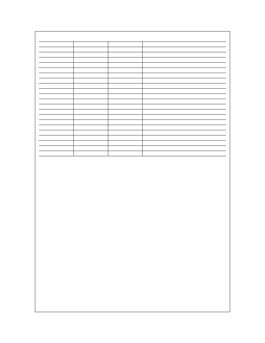
Parts List for Test Evaluation Board (RMBA19500A-TB, G654188/G654942)
Thermal Considerations for Heat Sinking the RMBA19500
The PWB must be prepared with either an embedded
copper slug in the board where the package is to be
mounted or a heat sink should be attached to the backside
of the PWB where the package is to be mounted on the
front side. The slug or the heat sink should be made of a
highly electrically and thermally conductive material such
as copper or aluminum. The slug should be at least the
same thickness as the PWB. In the case of the heat sink, a
small pedestal should protrude through a hole in the PWB
where the package bottom is directly soldered. In either
configuration, the top surface of the slug or the pedestal
should be made coplanar with the package lead mounting
plane i.e., the top surface of the PWB. Use Sn96 solder
(96.5% Sn and 3.5% Ag) at 220°C for 20 seconds or less to
attach the heat sink to the backside of the PWB. Then,
using Sn63, the package bottom should be firmly soldered
to the slug or the pedestal while the pins are soldered to the
respective pads on the front side of the PWB without
causing any stress on the pins. Remove flux completely if
used for soldering.
Part
Value
Size (EIA)
Vendor(s)
L1, L2, L4
5.6nH
.06" x .03"
Toko (LL1608-F5N6)
L3
10nH
.085" x .060"
Coilcraft (0805HT-10NTKBC)
C1
10pF
.067" x .036"
Murata (GRM39COG100J050AD)
C9
2.2pF
.042" x .022"
Murata (GRM36COG2R2J050BD)
C3, C4, C5
1500pF
.067" x .036"
Murata (GRM39Y5V152Z50V)
C10
2.0pF
Murata (GRM36COG2R20J050BD)
C2
15.0pF
.042" x .022"
Murata (GRM36COG150J050)
C8, C11, C14, C15
4.7µF
.134" x .071"
TDK (C3216XR1A475KT)
C6, C7
0.1µF
.183" x .054"
Murata (GRM39Y5V104Z50)
R1, R5
20
.069" x .037"
IMS (RCI-0603-20R0J)
R2, R7
1000
.069" x .037"
IMS (RCI-0603-1001J)
R3
910
.069" x .037"
IMS (RCI-0603-9100J)
R4
30
.069" x .037"
IMS (RCI-0603-30R0J)
R6
1.1K
.069" x .037"
IMS (RCI-0603-1101J)
R8
390
IMS (RCI-0603-3900J)
R9
300
IMS (RCI-0603-3000J)
U1
RMBA19500-58
.31" x .41"
Fairchild
HS
Heatsink
Fairchild, G655548
P1
Terminals
3M (2340-5211TN)
J1, J2
SMA Connectors
E.F. Johnson (142-0701-841)
Board
FR4
Fairchild Dwg# G654187/G654941