©2004 Fairchild Semiconductor Corporation
September 2004
RMPA0965 Rev. C
RMPA0965
RMPA0965
CDMA and CDMA2000-1X PowerEdgeTM Power Amplifier Module
General Description
The RMPA0965 power amplifier module (PAM) is designed
for cellular band AMPS, CDMA and CDMA2000-1X
applications. The 2 stage PAM is internally matched to 50
to minimize the use of external components and features a
low-power mode to reduce standby current and DC power
consumption during peak phone usage. High power-added
efficiency and excellent linearity are achieved using our
InGaP Heterojunction Bipolar Transistor (HBT) process.
Features
· Single positive-supply operation with low power and
shutdown modes
· 40% CDMA efficiency at +28 dBm average output power
· 52% AMPS mode efficiency at +31 dBm output power
· Compact LCC package ( 3.0 x 3.0 x 1.0 mm)
· Internally matched to 50
and DC blocked RF input/
output
· Meets CDMA2000-1XRTT performance requirements
Absolute Ratings
1
Note:
1:
No permanent damage with only one parameter set at extreme limit. Other parameters set to typical values.
Functional Block Diagram
Symbol
Parameter
Value
Units
Vcc1, Vcc2
Supply Voltages
5.0
V
Vref
Reference Voltage
2.6 to 3.5
V
Vmode
Power Control Voltage
3.5
V
Pin
RF Input Power
+10
dBm
T
STG
Storage Temperature
-55 to +150
°C
Vcc2
RF OUT
GND
GND
Vref
RF IN
Vcc1
(paddle ground on package bottom)
(Top View)
1
2
3
4
DC BIAS CONTROL
INPUT
MATCH
OUTPUT
MATCH
MMIC
Vmode
8
7
6
5
Device
©2004 Fairchild Semiconductor Corporation
RMPA0965 Rev. C
RMPA0965
Electrical Characteristics
1
Notes:
1:
All parameters met at Tc = +25°C, Vcc = +3.4V, Freq = 836.5MHz, Vref = 2.85V and load VSWR
1.2:1, unless otherwise noted.
2:
All phase angles.
Recommend Operating Conditions
Symbol
Parameter
Min
Typ
Max
Units
Comments
f
Operating Frequency
824
849
MHz
CDMA Operation
SSg
Small-Signal Gain
31
dB
Po = 0 dBm
Gp
Power Gain
30
29
dB
dB
Po = +28 dBm; Vmode = 0V
Po = +16 dBm; Vmode
2.0V
Po
Linear Output Power
28
16
dBm
dBm
Vmode = 0V
Vmode
2.0V
PAEd
PAE (digital) @ +28 dBm
40
%
Vmode = 0V
PAE (digital) @ +16 dBm
9
%
Vmode
2.0V
PAEd (digital) @ +16 dBm
25
%
Vmode
2.0V, Vcc = 1.4V
Itot
High Power Total Current
470
mA
Po = +28 dBm, Vmode = 0V
Low Power Total Current
120
mA
Po = +16 dBm, Vmode = 2.0V
Adjacent Channel Power Ratio
IS-95 A/B Modulation
ACPR1
±885 KHz Offset
-50
-52
dBc
dBc
Po = +28 dBm; Vmode = 0V
Po = +16 dBm; Vmode
2.0V
ACPR2
±1.98 MHz Offset
-60
-70
dBc
dBc
Po = +28 dBm; Vmode = 0V
Po = +16 dBm; Vmode
2.0V
AMPS Operation
Gp
Gain
30
dB
Po = +31 dBm
PAEa
Power-Added Efficiency (analog)
52
%
Po = +31 dBm
General Characteristics
VSWR
Input Impedance
2.0:1
2.5:1
NF
Noise Figure
4
dB
Rx No
Receive Band Noise Power
-137
dBm/Hz Po
+28 dBm; 869 to 894 MHz
2fo-5fo
Harmonic Suppression
-30
dBc
Po
+28 dBm
S
Spurious Outputs
2
-60
dBc
Load VSWR
5.0:1
Ruggedness w/ Load Mismatch
10:1
No permanent damage.
Tc
Case Operating Temperature
-30
85
°C
DC Characteristics
Iccq
Quiescent Current
55
mA
Vmode
2.0V
Iref
Reference Current
5
8
mA
Po
+28 dBm
Icc(off)
Shutdown Leakage Current
1
5
µA
No applied RF signal.
Symbol
Parameter
Min
Typ
Max
Units
f
Operating Frequency
824
849
MHz
Vcc1, Vcc2
Supply Voltage
3.0
3.4
4.2
V
Vref
Reference Voltage
(Operating)
(Shutdown)
2.7
0
2.85
3.1
0.5
V
V
Vmode
Bias Control Voltage
(low-power)
(high-power)
1.8
0
2.0
3.0
0.5
V
V
Pout
Linear Output Power
(high-power)
(low-power)
+28
+16
dBm
dBm
T
C
Case Operating Temperature
-30
+85
°C
©2004 Fairchild Semiconductor Corporation
RMPA0965 Rev. C
RMPA0965
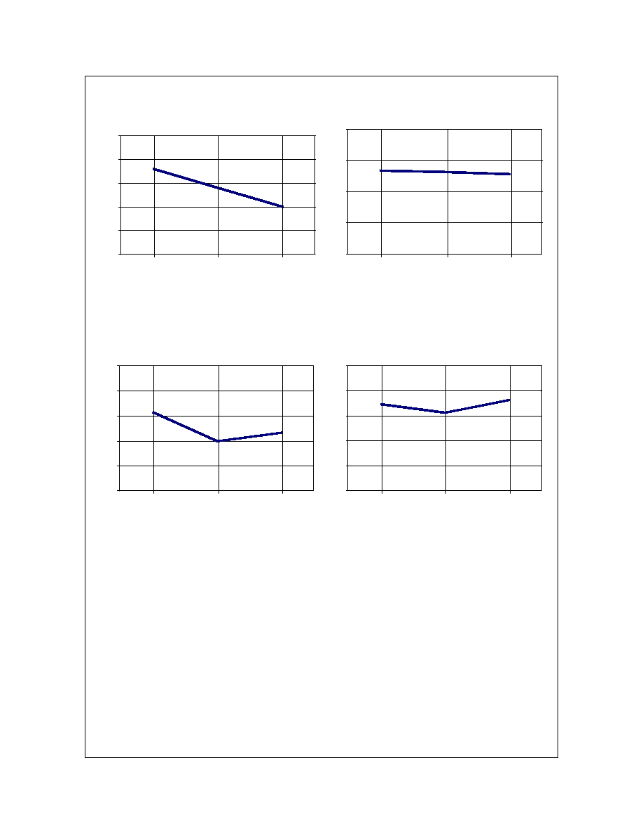
Typical Characteristics
RMPA0965 PAE vs. Frequency, IS95 Modulation
Pout = 28dBm, Vcc = 3.4V, Vref = 2.85V, Vmode = 0V, T
C
= 25
°C
RMPA0965
ACPR1
vs. Frequency, IS95 Modulation
Pout = 28dBm, Vcc = 3.4V, Vref = 2.85V, Vmode = 0V, T
C
= 25
°C
RMPA0965
ACPR2
vs. Frequency, IS95 Modulation
Pout = 28dBm, Vcc = 3.4V, Vref = 2.85V, Vmode = 0V, T
C
= 25
°C
RMPA0965 Gain vs. Frequency, IS95 Modulation
Pout = 28dBm, Vcc = 3.4V, Vref = 2.85V, Vmode = 0V, T
C
= 25
°C
37
38
39
40
41
42
824
836.5
849
FREQUENCY (MHz)
PAE (%)
28
29
30
31
32
824
836.5
849
FREQUENCY (MHz)
GAIN (dB)
-52
-51
-50
-49
-48
-47
824
836.5
849
FREQUENCY (MHz)
ACPR1 (dBc)
-62
-61
-60
-59
-58
-57
824
836.5
849
FREQUENCY (MHz)
ACPR2 (dBc)

©2004 Fairchild Semiconductor Corporation
RMPA0965 Rev. C
RMPA0965
Application Information
CAUTION: THIS IS AN ESD SENSITIVE DEVICE
Precautions to Avoid Permanent Device Damage:
· Cleanliness: Observe proper handling procedures to
ensure clean devices and PCBs. Devices should remain
in their original packaging until component placement to
ensure no contamination or damage to RF, DC & ground
contact areas.
· Device Cleaning: Standard board cleaning techniques
should not present device problems provided that the
boards are properly dried to remove solvents or water
residues.
· Static Sensitivity: Follow ESD precautions to protect
against ESD damage:
A properly grounded static-dissipative surface on
which to place devices.
Static-dissipative floor or mat.
A properly grounded conductive wrist strap for each
person to wear while handling devices.
· General Handling: Handle the package on the top with a
vacuum collet or along the edges with a sharp pair of
bent tweezers. Avoiding damaging the RF, DC, & ground
contacts on the package bottom. Do not apply excessive
pressure to the top of the lid.
· Device Storage: Devices are supplied in heat-sealed,
moisture-barrier bags. In this condition, devices are
protected and require no special storage conditions.
Once the sealed bag has been opened, devices should
be stored in a dry nitrogen environment.
Device RF:
Fairchild RF recommends the following procedures prior to
assembly.
· Dry-bake devices at 125°C for 24 hours minimum. Note:
The shipping trays cannot withstand 125°C baking
temperature.
· Assemble the dry-baked devices within 7 days of
removal from the oven.
· During the 7-day period, the devices must be stored in an
environment of less than 60% relative humidity and a
maximum temperature of 30°C
· If the 7-day period or the environmental conditions have
been exceeded, then the dry-bake procedure must be
repeated.
Solder Materials & Temperature Profile:
Reflow
soldering is the preferred method of SMT attachment. Hand
soldering is not recommended.
· Reflow Profile
Ramp-up: During this stage the solvents are
evaporated from the solder paste. Care should be
taken to prevent rapid oxidation (or paste slump) and
solder bursts caused by violent solvent out-gassing. A
typical heating rate is 1- 2°C/sec.
Pre-heat/soak: The soak temperature stage serves
two purposes; the flux is activated and the board and
devices achieve a uniform temperature. The
recommended soak condition is: 120-150 seconds at
150°C.
Reflow Zone: If the temperature is too high, then
devices may be damaged by mechanical stress due to
thermal mismatch or there may be problems due to
excessive solder oxidation. Excessive time at
temperature can enhance the formation of inter-
metallic compounds at the lead/board interface and
may lead to early mechanical failure of the joint.
Reflow must occur prior to the flux being completely
driven off. The duration of peak reflow temperature
should not exceed 10 seconds. Maximum soldering
temperatures should be in the range 215-220°C, with
a maximum limit of 225°C.
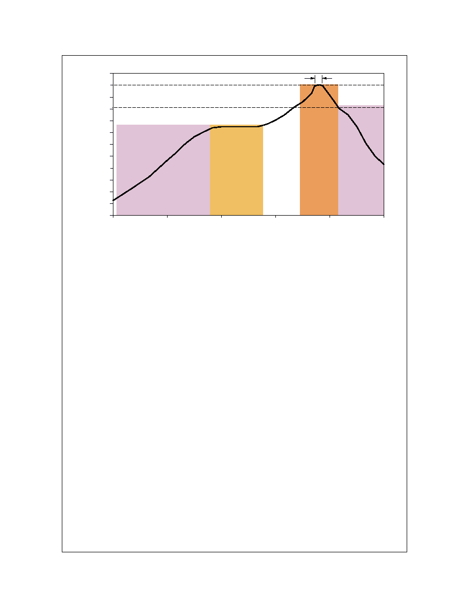
Cooling Zone: Steep thermal gradients may give rise
to excessive thermal shock. However, rapid cooling
promotes a finer grain structure and a more crack-
resistant solder joint. The illustration below indicates
the recommended soldering profile.
Solder Joint Characteristics:
Proper operation of this device depends on a reliable void-
free attachment of the heatsink to the PWB. The solder joint
should be 95% void-free and be a consistent thickness.
Rework Considerations:
Rework of a device attached to a board is limited to reflow
of the solder with a heat gun. The device should not be
subjected to more than 225°C and reflow solder in the
molten state for more than 5 seconds. No more than 2
rework operations should be performed.