 | ÐлекÑÑоннÑй компоненÑ: RMPA2265 | СкаÑаÑÑ:  PDF PDF  ZIP ZIP |
Äîêóìåíòàöèÿ è îïèñàíèÿ www.docs.chipfind.ru

©2004 Fairchild Semiconductor Corporation
December 2004
RMPA2265 Rev.
E
RMPA2265
2265
PYWW
RMPA2265
Dual Band WCDMA Power Amplifier Module
1850 to 1910 MHz and 1920 to 1980 MHz
General Description
The RMPA2265 power amplifier module (PAM) is designed
for WCDMA applications in both the 18501910 and 1920
1980 MHz bands. The 2 stage PAM is internally matched to
50
to minimize the use of external components and
features a low-power mode to reduce standby current and
DC power consumption during peak phone usage. High
power-added efficiency and excellent linearity are achieved
using Fairchild's InGaP/GaAs Heterojunction Bipolar
Transistor (HBT) process.
Features
· Single positive-supply operation and low power and
shutdown modes
· 42% WCDMA efficiency at +28 dBm average output
power 19201980 MHz
· 39% WCDMA efficiency at 27.5 dBm average output
power 18501910 MHz
· Meets UMTS/WCDMA performance requirements in
both UMTS bands
· Compact, low-profile package(3.0 x 3.0 x 1.0 mm
nominal)
· Internally matched to 50
and DC blocked RF input/
output
Functional Block Diagram
Device (3 x 3 x 1mm)
PA MODULE
(paddle ground on package bottom)
4
3
2
1
8
7
6
5
DC Bias Control
Input
Match
Output
Match
Vcc2
RF OUT
GND
Vref
RF IN
Vcc1
MMIC
(Top View)
Vmode
GND

©2004 Fairchild Semiconductor Corporation RMPA2265 Rev.
E
RMPA2265
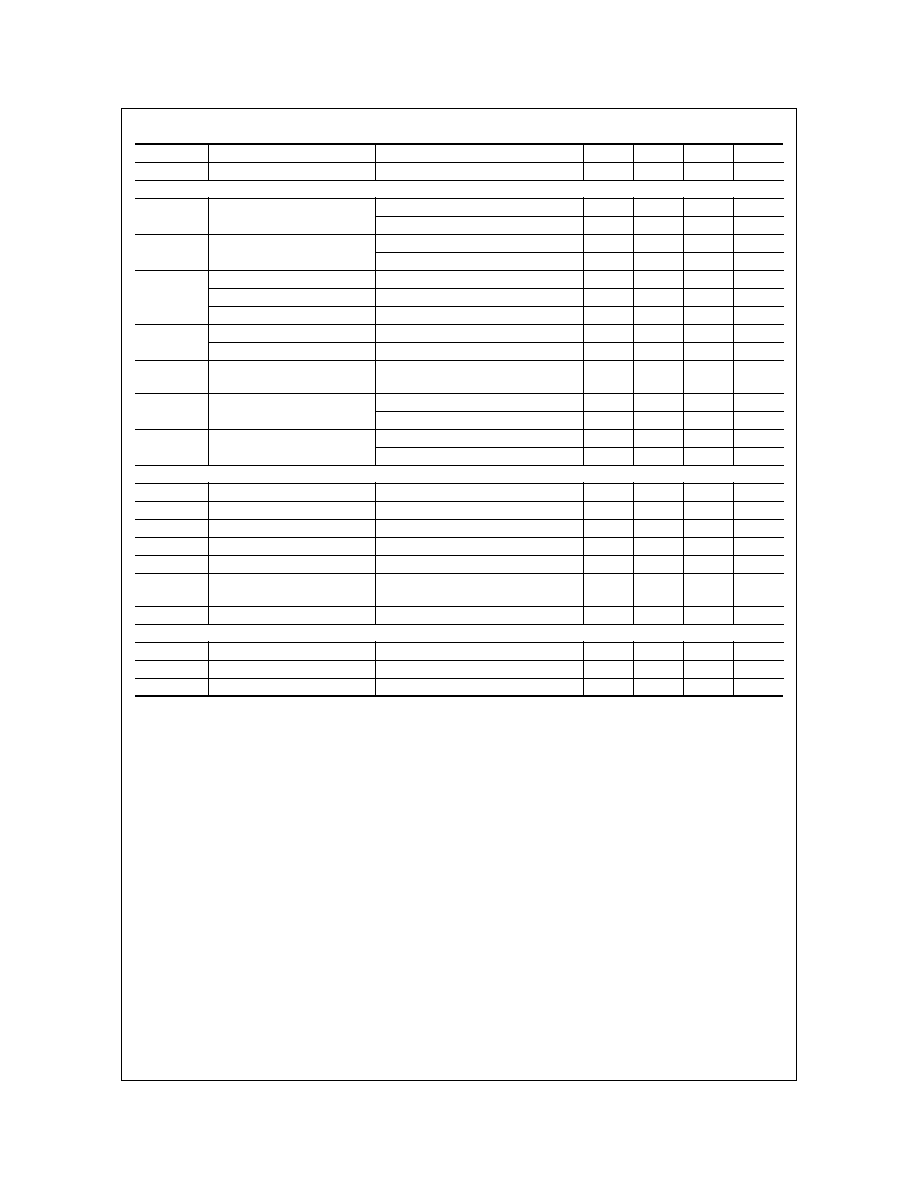
Absolute Ratings
1
Note:
1:
No permanent damage with only one parameter set at extreme limit. Other parameters set to typical values.
Electrical Characteristics (1920 to 1980 MHz)
1
Notes:
1:
All parameters met at T
C
= +25°C, V
CC
= +3.4V, V
REF
= 2.85V and load VSWR
1.2:1, unless otherwise noted.
2:
All phase angles
3:
Guaranteed by design
Symbol
Parameter
Ratings
Units
V
CC1
, V
CC2
Supply Voltages
5.0
V
V
REF
Reference Voltage
2.6 to 3.5
V
V
MODE
Power Control Voltage
3.5
V
P
IN
RF Input Power
+10
dBm
T
STG
Storage Temperature
-55 to +150
°C
Symbol
Parameter
Comments
Min
Typ
Max
Units
f
Operating Frequency
1920
1980
MHz
WCDMA Operation
Gp
Power Gain
Po = +28dBm, Vmode = 0V
26
28
dB
Po = +16dBm, Vmode
2.0V
26
dB
Po
Linear Output Power
Vmode = 0V
28
dBm
Vmode
2.0V
16
dBm
PAEd
PAEd (digital) @ +28dBm
Vmode = 0V
42
%
PAEd (digital) @ +16dBm
Vmode
2.0V
9
%
PAEd (digital) @ +16dBm
Vmode
2.0V, Vcc = 1.4V
25
%
Itot
High Power Total Current
Po = +28dBm, Vmode = 0V
440
mA
Low Power Total Current
Po = +16dBm, Vmode = 2.0V
120
mA
Adjacent Channel Leakage
Ratio
ACLR1
±5.00MHz Offset
19201980 MHz
Po = +28dBm, Vmode = 0V
-40
dBc
Po = +16dBm, Vmode
2.0V
-42
dBc
ACLR2
±10.00MHz Offset
19201980 MHz
Po = +28dBm, Vmode = 0V
-54
dBc
Po = +16dBm, Vmode
2.0V
-66
dBc
General Characteristics
VSWR
Input Impedance
2.0:1
NF
Noise Figure
4
dB
Rx No
Receive Band Noise Power
Po
+28dBm, 2110 to 2170 MHz
-139
dBm/Hz
2fo 5fo
Harmonic Suppression
Po
+28dBm
-50
dBc
S
Spurious Outputs
2, 3
Load VSWR
5.0:1
-60
dBc
Ruggedness with Load
Mismatch
3
No permanent damage
10:1
Tc
Case Operating Temperature
-30
85
°C
DC Characteristics
Iccq
Quiescent Current
Vmode
2.0V
50
mA
Iref
Reference Current
Po
+28dBm
5
mA
Icc(off)
Shutdown Leakage Current
No applied RF signal
1
5
µA
©2004 Fairchild Semiconductor Corporation RMPA2265 Rev.
E
RMPA2265
Electrical Characteristics (1850 to 1910 MHz)
1
Notes:
1:
All parameters met at T
C
= +25°C, V
CC
= +3.4V, V
REF
= 2.85V and load VSWR
1.2:1, unless otherwise noted.
2:
All phase angles
3:
Guaranteed by design
Symbol
Parameter
Comments
Min
Typ
Max
Units
f
Operating Frequency
1850
1910
MHz
WCDMA Operation
Gp
Power Gain
Po = +27.5dBm, Vmode = 0V
26
28
dB
Po = +16dBm, Vmode
2.0V
26
dB
Po
Linear Output Power
Vmode = 0V
27.5
dBm
Vmode
2.0V
16
dBm
PAEd
PAEd (digital) @ +27.5dBm
Vmode = 0V
39
%
PAEd (digital) @ +16dBm
Vmode
2.0V
9
%
PAEd (digital) @ +16dBm
Vmode
2.0V, Vcc = 1.4V
25
%
Itot
High Power Total Current
Po = +27.5dBm, Vmode = 0V
420
mA
Low Power Total Current
Po = +16dBm, Vmode = 2.0V
120
mA
Adjacent Channel Leakage
Ratio
ACLR1
±5.00MHz Offset
18501910 MHz
Po = +27.5dBm, Vmode = 0V
-40
dBc
Po = +16dBm, Vmode
2.0V
-42
dBc
ACLR2
±10.00MHz Offset
18501910 MHz
Po = +27.5dBm, Vmode = 0V
-54
dBc
Po = +16dBm, Vmode
2.0V
-66
dBc
General Characteristics
VSWR
Input Impedance
2.0:1
NF
Noise Figure
4
dB
Rx No
Receive Band Noise Power
Po
+27.5dBm, 2110 to 2170 MHz
-139
dBm/Hz
2fo 5fo
Harmonic Suppression
Po
+27.5dBm
-50
dBc
S
Spurious Outputs
2, 3
Load VSWR
5.0:1
-60
dBc
Ruggedness with Load
Mismatch
3
No permanent damage
10:1
Tc
Case Operating Temperature
-30
85
°C
DC Characteristics
Iccq
Quiescent Current
Vmode
2.0V
50
mA
Iref
Reference Current
Po
+27.5dBm
5
mA
Icc(off)
Shutdown Leakage Current
No applied RF signal
1
5
µA

©2004 Fairchild Semiconductor Corporation RMPA2265 Rev.
E
RMPA2265
Recommended Operating Conditions
Symbol
Parameter
Min
Typ
Max
Units
f
Operating Frequency
1850
1980
MHz
V
CC1
, V
CC2
Supply Voltage
3.0
3.4
4.2
V
V
REF
Reference Voltage
Operating
Shutdown
2.7
0
2.85
3.1
0.5
V
V
V
MODE
Bias Control Voltage
Low-Power
High-Power
1.8
0
2.0
3.0
0.5
V
V
P
OUT
Linear Output Power (low-power)
19201980 MHz (high power)
18501910 MHz (high power)
+16
+28
+27.5
dBm
dBm
dBm
T
C
Case Operating Temperature
-30
+85
°C
Package Outline
Signal Description
Pin #
Signal Name
Description
1
VCC1
Supply Voltage to Input Stage
2
RF In
RF Input Signal
3
VMODE
High Power/Low Power Switch
4
VREF
Reference Voltage
5
GND
Ground
6
GND
Ground
7
RF Out
RF Output Signal
8
VCC2
Supply Voltage to Output Stage
9
GND
Ground
1
2
3.00
±0.10mm
SQUARE
0.60mm
MOLD HEAD HEIGHT
1.00
±0.10mm
0.44
FRONT VIEW
TOP VIEW
I/O 1 INDICATOR
3
4
8
2265
PYWW
7
6
5
©2004 Fairchild Semiconductor Corporation RMPA2265 Rev.
E
RMPA2265
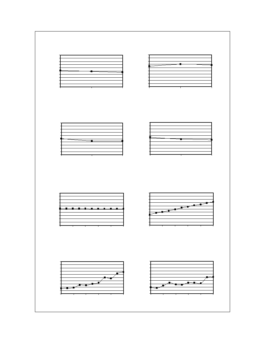
Performance Data: 1920 to 1980 MHz
RMPA2265 3x3 WCDMA PA , Freq=1.95GHz
Vcc=3.4V, Vref=2.85V, Vmode=0V
23.0
24.0
25.0
26.0
27.0
28.0
29.0
30.0
31.0
32.0
33.0
27.0
27.2
27.4
27.6
27.8
28.0
Pout (dBm)
Gain (dB)
RMPA2265 3x3 WCDMA PA , Freq=1.95GHz
Vcc=3.4V, Vref=2.85V, Vmode=0V
35.0
36.0
37.0
38.0
39.0
40.0
41.0
42.0
43.0
44.0
45.0
27.0
27.2
27.4
27.6
27.8
28.0
Pout (dBm)
PAE (%)
RMPA2265 3x3 WCDMA PA , Freq=1.95GHz
Vcc=3.4V, Vref=2.85V, Vmode=0V
-47.0
-46.0
-45.0
-44.0
-43.0
-42.0
-41.0
-40.0
-39.0
-38.0
-37.0
27.0
27.2
27.4
27.6
27.8
28.0
Pout (dBm)
ACLR1 (dBc)
RMPA2265 3x3 WCDMA PA , Freq=1.95GHz
Vcc=3.4V, Vref=2.85V, Vmode=0V
-60.0
-59.0
-58.0
-57.0
-56.0
-55.0
-54.0
-53.0
-52.0
-51.0
-50.0
27.0
27.2
27.4
27.6
27.8
28.0
Pout (dBm)
ACLR2 (dBc)
RMPA2265 3x3 WCDMA PA
Vcc=3.4V, Vref=2.85V, Vmode=0V, Pout=28dBm
23.0
24.0
25.0
26.0
27.0
28.0
29.0
30.0
31.0
32.0
33.0
1920
1950
1980
Frequency (MHz)
Gain (dB)
RMPA2265 3x3 WCDMA PA
Vcc=3.4V, Vref=2.85V, Vmode=0V, Pout=28dBm
35.0
36.0
37.0
38.0
39.0
40.0
41.0
42.0
43.0
44.0
45.0
1920
1950
1980
Frequency (MHz)
PAE (%)
RMPA2265 3x3 WCDMA PA
Vcc=3.4V, Vref=2.85V, Vmode=0V, Pout=28dBm
-50.0
-48.0
-46.0
-44.0
-42.0
-40.0
-38.0
-36.0
-34.0
-32.0
-30.0
1920
1950
1980
Frequency (MHz)
ACLR1 (dBc)
RMPA2265 3x3 WCDMA PA
Vcc=3.4V, Vref=2.85V, Vmode=0V, Pout=28dBm
-65.0
-63.0
-61.0
-59.0
-57.0
-55.0
-53.0
-51.0
-49.0
-47.0
-45.0
1920
1950
1980
Frequency (MHz)
ACLR2 (dBc)