 | ÐлекÑÑоннÑй компоненÑ: RMPA2458 | СкаÑаÑÑ:  PDF PDF  ZIP ZIP |
Äîêóìåíòàöèÿ è îïèñàíèÿ www.docs.chipfind.ru
©2005 Fairchild Semiconductor Corporation
1
www.fairchildsemi.com
March 2005
RMPA2458 Rev. C
RMP
A2458 2.42.5 GHz InGaP HBT Lo
w Current Linear P
o
wer Amplifier
RMPA2458
2.42.5 GHz InGaP HBT Low Current Linear Power Amplifier
Features
31.5dB small signal gain
27dBm output power @ 1dB compression
103mA total current at 19dBm modulated power out
2.5% EVM at 19 dBm modulated power out
3.3V collector supply operation
2.9V mirror supply operation
Power saving shutdown options (bias control)
Integrated power detector with 20dB dynamic range
Lead-free RoHS compliant 3 x 3 x 0.9mm leadless package
Internally matched to 50 Ohms and DC blocked RF input/
output
Optimized for use in 802.11b/g applications
General Description
The RMPA2458 power amplifier is designed for high
performance WLAN applications in the 2.42.5 GHz frequency
band. The low profile 16 pin 3 x 3 x 0.9 mm package with internal
matching on both input and output to 50 Ohms minimizes next
level PCB space and allows for simplified integration. The on-
chip detector provides power sensing capability while the bias
control provides power saving shutdown capability. The PA's
industry leading low power consumption and excellent linearity
are achieved using our InGaP Heterojunction Bipolar Transistor
(HBT) technology.
Device
Electrical Characteristics
1
802.11g OFDM Modulation
(176 µs burst time, 100 µs idle time) 54 Mbps Data Rate, 16.7 MHz Bandwidth
Notes:
1. VC1, VC2, VC3 = 3.3V, VM123 = 2.9V, T
A
= 25°C, PA is constantly biased, 50
system.
2. Percentage includes system noise floor of EVM = 0.8%.
3. P
OUT
measured at P
IN
corresponding to power detection threshold.
Parameter
Min
Typ
Max
Units
Frequency
2.4
2.5
GHz
Collector Supply Voltage
3.0
3.3
3.6
V
Mirror Supply Voltage
2.9
V
Mirror Supply Current
3.3
mA
Gain
31.5
dB
Total Current @ 19dBm P
OUT
103
mA
EVM @ 19dBm P
OUT
2
2.5
%
Detector Output @ 19dBm P
OUT
340
mV
Detector Threshold
3
5
dBm
Preliminary
2
www.fairchildsemi.com
RMPA2458 Rev. C
RMP
A2458 2.42.5 GHz InGaP HBT Lo
w Current Linear P
o
wer Amplifier
Electrical Characteristics
1
802.11b CCK Modulation
(RF not framed) 11 Mbps Data Rate 22.0 MHz Bandwidth
Electrical Characteristics
1
Single Tone
Notes:
1. VC1, VC2, VC3 = 3.3V, VM123 = 2.9 Volts, Ta = 25°C, P
A
is constantly biased, 50
system.
2. P
IN
is adjusted to point where performance approaches spectral mask requirements.
3. P
OUT
measured at P
IN
corresponding to power detection threshold.
4. Mirror bias current is included in the total quiescent current.
5. Measured from Device On signal turn on to the point where RF P
OUT
stabilizes to 0.5dB.
6. Load VSWR is set to 8:1 and the angle is varied 360 degrees. P
OUT
= -30dBm to P1dB.
Parameter
Min
Typ
Max
Units
Frequency 2.4
2.5
GHz
Collector Supply Voltage
3.0
3.3
3.6
V
Mirror Supply Voltage
2.9
V
Mirror Supply Current
3.3
mA
Gain
32
dB
Total Current @ 19dBm Pout
130
mA
First Side Lobe Power @ 19dBm Pout
-36
dBm
Second Side Lobe Power @ 19dBm Pout
-60
dBm
Max Pout Spectral Mask Compliance
2
24
dBm
Detector Output @ 19dBm Pout
1.15
V
Detector Pout Threshold
3
5
dBm
Parameter
Min
Typ
Max
Units
Frequency 2.4
2.5
GHz
Collector Supply Voltage
3.0
3.3
3.6
V
Mirror Supply Voltage (VM123)
2.6
2.9
3.1
V
Gain
31.5
dB
Total Quiescent Current
49
mA
Bias Current at pin VM123
4
3.2
mA
P1dB Compression
27
dBm
Current @ P1dB Compression
600
mA
Shutdown Current (VM123 = 0V)
<1.0
µA
Input Return Loss
12
dB
Output Return Loss
9
dB
Detector Output at P1dB Compression
2.4
V
Detector Pout Threshold
3
5
V
Turn-on Time
5
<1.0
µS
Spurious (Stability)
6
-65
dBc
3
www.fairchildsemi.com
RMPA2458 Rev. C
RMP
A2458 2.42.5 GHz InGaP HBT Lo
w Current Linear P
o
wer Amplifier
Absolute Ratings
1
Note:
1. No permanent damage with one parameter set at extreme limit. Other parameters set to typical values.
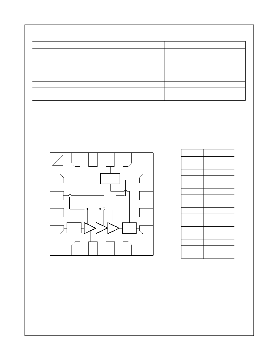
Functional Block Diagram
Symbol
Parameter
Ratings
Units
VC1, VC2, VC3
Positive Supply Voltage
5
V
IC1, IC2, IC3
Supply Current
IC1
IC2
IC3
50
150
700
mA
mA
mA
VM123
Positive Bias Voltage
3.6
V
P
IN
RF Input Power
+5
dBm
T
CASE
Case Operating Temperature
-40 to +85
°C
T
STG
Storage Temperature
-55 to +150
°C
12
8
VC3
11
N/C
10
GND
9
1
2
3
4
RF OUT
VM123
VC2
GND
RF IN
GND
7
VDET
6
GND
5
13
14
15
16
GND
GND
GND
VC1
GND
VOLTAGE
DETECTOR
OUTPUT
MATCH
INPUT
MATCH
Pin
Description
1
VM123
2
VC2
3
GND
4
RF IN
5
GND
6
VC1
7
GND
8
GND
9
RF OUT
10
GND
11
N/C
12
VC3
13
GND
14
VDET
15
GND
16
GND
4
www.fairchildsemi.com
RMPA2458 Rev. C
RMP
A2458 2.42.5 GHz InGaP HBT Lo
w Current Linear P
o
wer Amplifier
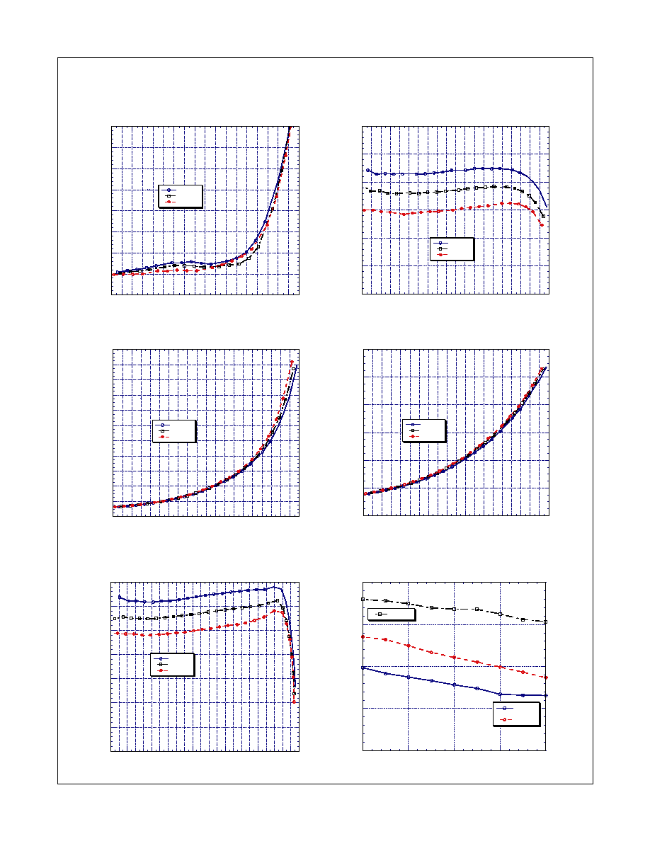
Performance Data
802.11g OFDM Modulation
(176 µs burst time, 100 µs idle time) 54 Mbps Data Rate, 16.7 MHz Bandwidth
0
1
2
3
4
5
6
7
8
5
7
9
11
13
15
17
19
21
23
Total Measured EVM Vs. Modulated Power Out
VC=3.3V VM=2.9V T=25
°C
Modulated Power Out (dBm)
Modulated Power Out (dBm)
26
27
28
29
30
31
32
33
5
7
9
11
13
15
17
19
21
23
25
27
Gain Vs. Single Tone Power Out
VC=3.3V VM=2.9V T=25
°C
Single Tone Power Out (dBm)
15
20
25
30
35
-20
-15
-10
-5
0
2.35
2.4
2.45
2.5
2.55
S-Parameters Vs. Frequency
VC=3.3V VM=2.9V T=25
°C
Frequency (GHz)
S21 (dB)
Gain (dB)
Detector Voltage (mV)
Total Current (mA)
Gain (dB)
Total Measured MVE (%)
S11, S22 (dB)
200
400
600
800
1000
1200
1400
5
7
9
11
13
15
17
19
21
23
25
Detector Voltage Vs. Modulated Power Out
VC=3.3V VM=2.9V T=25
°C
260
240
220
200
180
160
140
120
100
80
60
40
5
7
9
11
13
15
17
19
21
23
25
Total Current Vs. Modulated Power Out
VC=3.3V VM=2.9V T=25
°C
28
29
30
31
32
33
34
5
7
9
11
13
15
17
19
21
23
25
Gain Vs. Modulated Power Out
VC=3.3V VM=2.9V T=25
°C
Modulated Power Out (dBm)
Modulated Power Out (dBm)
Note: Uncorrected EVM. Source EVM is approximately 0.8%.
S21 (dB)
S11 (dB)
S22 (dB)
2.40 GHz
2.45 GHz
2.50 GHz
2.40 GHz
2.45 GHz
2.50 GHz
2.40 GHz
2.45 GHz
2.50 GHz
2.40 GHz
2.45 GHz
2.50 GHz
2.40 GHz
2.45 GHz
2.50 GHz
Single Tone
5
www.fairchildsemi.com
RMPA2458 Rev. C
RMP
A2458 2.42.5 GHz InGaP HBT Lo
w Current Linear P
o
wer Amplifier
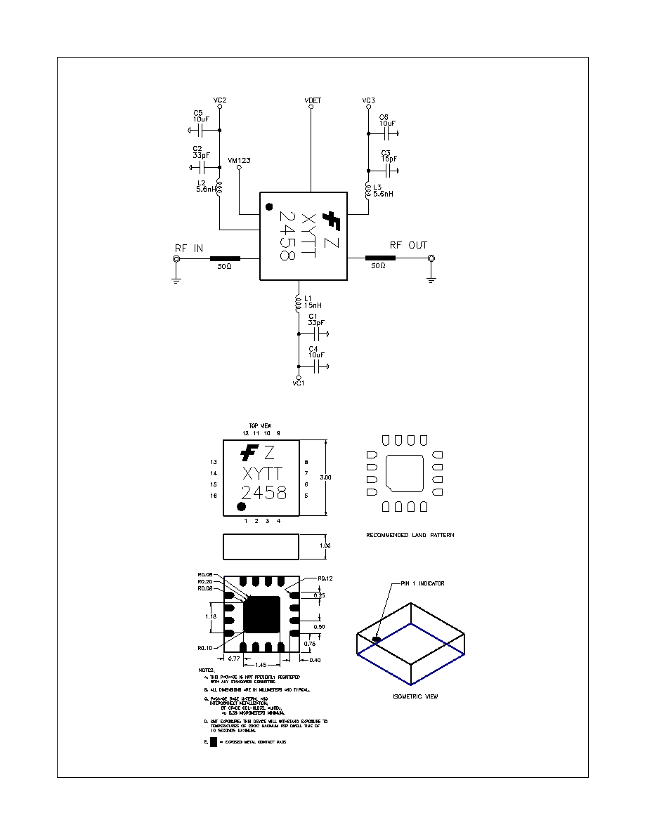
Evaluation Board Schematic
Package Outline
Backside Ground
16
1
2
3
4
12
11
10
9
15
14
13
5
6
7
8
Dimensions in mm
Note: Dimensions do not include protrusions or mold flash. These are not to exceed 0.006" (.155mm) on any side.