 | ÐлекÑÑоннÑй компоненÑ: RMPA61810 | СкаÑаÑÑ:  PDF PDF  ZIP ZIP |
Äîêóìåíòàöèÿ è îïèñàíèÿ www.docs.chipfind.ru
©2004 Fairchild Semiconductor Corporation
March 2004
RMPA61810 Rev. B
RMPA61810
RMPA61810
Single Channel 6-18 GHz 1 Watt Power Amplifier MMIC
General Description
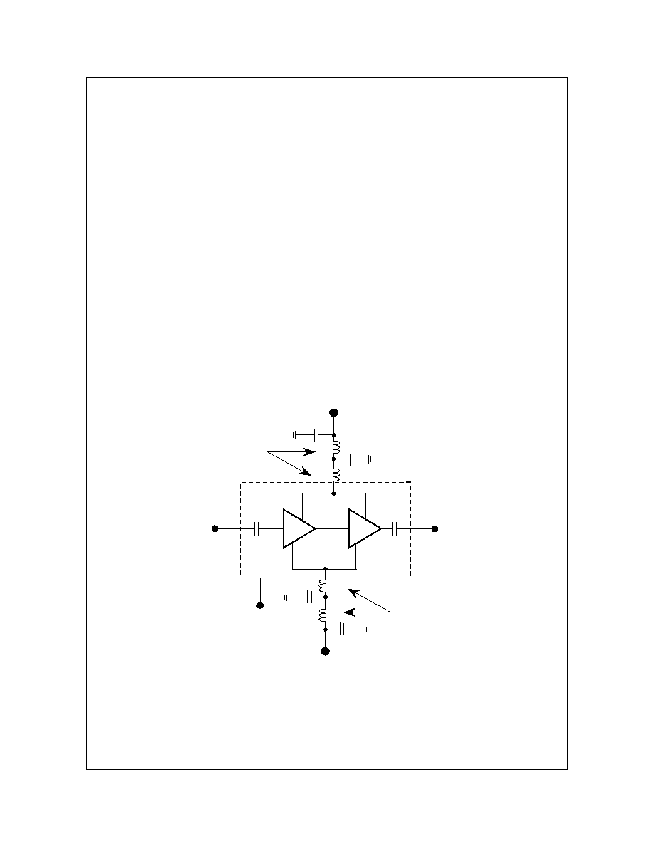
The Fairchild Semiconductor RMPA61810 is a fully
monolithic power amplifier operating over the 6.0 to 18.0
GHz frequency band. The amplifier uses a 0.25 micron
Pseudomorphic High Electron Mobility Transistor (PHEMT)
process to maximize efficiency and output power. The chip
configuration incorporates two stages of reactively
combined amplifiers at the output preceded by an input
amplifier stage. This single channel amplifier provides
typically, 21dB small signal gain and 31dBm output power
at 1dB gain compression.
Features
· 21dB Typical Small Signal Gain
· 2.0:1 Typical Input VSWR, 2.5:1 Typical Output VSWR
· 31dBm Output Power at 1dB Gain Compression
· 32dBm Output Power at 3dB Gain Compression
· 22% Typical Power Added Efficiency at 1dB Gain
Compression
· Chip size: 6.55mm x 2.67mm x 0.1mm
Absolute Ratings
Electrical Characteristics
(Operated at 25°C, 50
system, Vd = +8V, quiescent current (Idq = 600 mA)
Note:
1. Typical range of the negative gate voltage is -1 to 0V to set a typical Idq of 600 mA.
Symbol
Parameter
Ratings
Units
Vd
Positive Drain DC Voltage
8.5
V
Vg
Negative DC Voltage
-2
V
Vdg
Simultaneous (VdVg)
+10.5
V
Pin
RF CW Input Power (50
source)
27
dBm
Id
Drain Current
1.2
A
T
STG
Storage Temperature
-55 to +125
°C
Tc
Operating Baseplate Temperature
-40 to +85
°C
R
JC
Thermal Resistance (Channel to Backside)
12
°C/W
Parameter
Min
Typ
Max
Units
Frequency Range
6.0
18.0
GHz
Small Signal Gain
15
21
dB
P1dB Compression
28
31
dBm
P3dB Compression
30
32
dBm
PAE at 1dB Gain Compression
12
22
%
Input Return Loss
9.5
dB
Output Return Loss
7.4
dB
Gate Voltage (Vg)
1
-0.4
V
Gain vs. Temp. 0 ~ 85°C
-0.025
dB/°C
Device

©2004 Fairchild Semiconductor Corporation
RMPA61810 Rev. B
RMPA61810
Application Information
CAUTION: THIS IS AN ESD SENSITIVE DEVICE
Chip carrier material should be selected to have GaAs
compatible thermal coefficient of expansion and high
thermal conductivity such as copper molybdenum or
copper tungsten. The chip carrier should be machined,
finished flat, plated with gold over nickel and should be
capable of withstanding 325°C for 15 minutes.
Die attachment for power devices should utilize Gold/Tin
(80/20) eutectic alloy solder and should avoid hydrogen
environment for PHEMT devices. Note that the backside of
the chip is gold plated and is used as RF and DC Ground.
These GaAs devices should be handled with care and
stored in dry nitrogen environment to prevent
contamination of bonding surfaces. These are ESD
sensitive devices and should be handled with appropriate
precaution including the use of wrist-grounding straps. All
die attach and wire/ribbon bond equipment must be well
grounded to prevent static discharges through the device.
Recommended wire bonding uses 3 mils wide and 0.5 mil
thick gold ribbon with lengths as short as practical allowing
for appropriate stress relief. The RF input and output bonds
should be typically 0.012" long corresponding to a typical 2
mil gap between the chip and the substrate material.
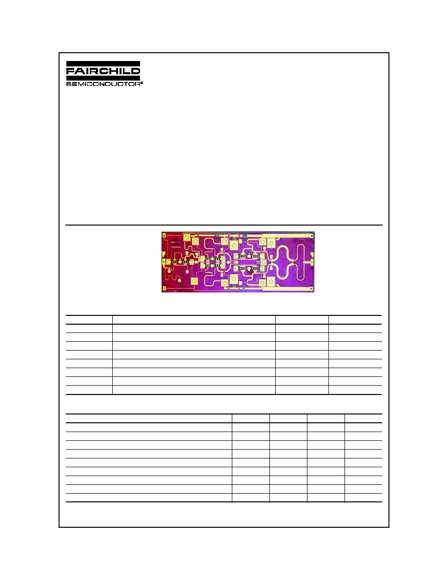
Figure 1. Functional Block Diagram
Figure 2. Chip Layout and Bond Pad Locations
(Chip size = 6.55mm x 2.67mm x 100µm. Back of Chip is RF and DC Ground)
Vg
Vg
Vd
Vd
RF IN
RF OUT
VG
0.0
105.3
5.8
13.2
48.1
59.5
94.4
5.8
13.2
48.1
59.5
94.4
101.8
101.8
VG
Dimension in mils
RMPA61810
8.7
8.0
249.3 254.8
2.4
249.3 254.8
3.3
0.0
258.0
RF
IN
VD
VD
RF
OUT
©2004 Fairchild Semiconductor Corporation
RMPA61810 Rev. B
RMPA61810
Application Note
Scope:
This application note briefly describes the procedure for
evaluating the Fairchild Semiconductor RMPA61810, high
efficiency 0.25µm PHEMT Single-Channel Amplifier. The
chip configuration incorporates two stages of reactively
combined amplifiers at the output preceded by an input
amplifier stage.
Carrier Assembly:
The attached drawing shows a recommended off chip bias
scheme for the RMPA61810. The MMIC is mounted on a
Cu shim or ridge, which in turn blazed to Cu-Mo-Cu, or Cu-
W, or Mo carrier with alumina 50
microstrip lines for in/out
RF connections and off-chip DC bias components. The
drawing shows the placement of components and bond
wire connections. The following should be noted:
(1) 1 mil gold bond wires are used on the carrier assembly.
(2) Use 3-1 mil gold wires about 25 mils in length for
optimum RF performance.
(3) Vg: Gate Voltage (negative) input terminal for amplifier
stages. For best results, the gate supply should have a
source resistance less than 100
.
(4) Vd: Drain Voltage (positive) input terminal for amplifier
stages.
(5) Vg and Vd on both sides of the MMIC must be biased to
insure proper operation.
(6) Bias decoupling capacitors of 0.01 µF (multilayer) and
100 pF (single layer) are used on the carrier.
(7) Close placement of external components is essential to
stability.
(8) The test fixture may require a pair of 25µF capacitor on
the drain and gate(optional) bias terminals to prevent
oscillations caused by the test fixture connections.
(9) For Laboratory testing, use good power supplies. Set
current limits on supplies to RF drive-up current level.
Keep supply wire/leads as short as possible and if
required use additional bypass capacitors at the fixture
terminals.
Figure 3. Recommended Application Schematic Circuit Diagram
DRAIN SUPPLY
(Vd = +8V)*
GATE SUPPLY (Vg)*
*Vg and Vd on both sides of the MMIC must be biased to insure proper operation.
10,000pF
100pF
100pF
10,000pF
GROUND
(Back of Chip)
Bond Wire Ls
Bond Wire Ls
MMIC CHIP
RF IN
RF OUT
L
L
L
L
©2004 Fairchild Semiconductor Corporation
RMPA61810 Rev. B
RMPA61810
Figure 4. Recommended Assembly and Bonding Diagram
Recommended Procedure for Biasing and Operation
CAUTION: LOSS OF GATE VOLTAGE (Vg) WHILE DRAIN VOLTAGE (Vd) IS PRESENT MAY DAMAGE THE
AMPLIFIER. THIS AMPLIFIER IS AN ESD SENSITIVE DEVICE.
VG
VG
VG
RF
IN
VD
VG
VD
VD
VD
RF OUT
RF IN
0.001" x 0.005" or 0.002" x 0.004" Au Ribbon,
4 Places
100pF Capacitor, 0.015" x 0.015" x 0.005",
4 Places
0.001" Dia. Au Wire, Typ.
50
, 0.015" TH Alumina Substrate,
2 Places
0.010" TH Cu Shim or Ridge
0.025" TH Cu-Mo-Cu or Cu-W Carrier
0.020" x 0.050" x 0.005" Stand-Off,
4 Places
0.01
µF Capacitor, 0.063" x 0.031" x 0.031",
4 Places
RMPA61810
RF
OUT
The following procedure must be followed to properly test
the amplifier:
Step 1:
Slowly apply Gate Voltage (typical Vpinch-off =
-1.5V) to terminal Vg.
Step 2:
Slowly apply Drain Voltage at Vd (<+5 volts) and
monitor drain current Ids. Adjust negative voltage Vg to set
the drain current (Ids) to approximately 600 mA. Adjust the
drain voltage Vg to nominal +8 volts (adjust Gate Voltage
Vg, if needed, to maintain the drain current at Ids.
Step 3:
After the bias condition is established, RF input
signal may now be applied at the appropriate frequency
band.
Step 4:
Follow Turn-off sequence:
(i) RF input power = off,
(ii) Vd = off,
(iii) Vg = off.
©2004 Fairchild Semiconductor Corporation
RMPA61810 Rev. B
RMPA61810
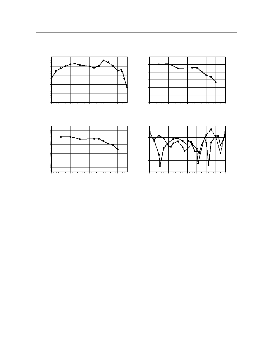
Typical Characteristics
The above data is derived from fixtured measurements which includes 3 parallel, 1 mil diameter, 15 mil long, gold bond wires
connected to the RF input and output.
The Id @ 1 dB compression increases to approximately 1A. The DC supply should be able to support the required current
to achieve the above performance.
0
5
10
15
20
25
4
6
8
10
12
14
16
18
20
10
12
14
16
18
20
FREQUENCY (GHz)
FREQUENCY (GHz)
FREQUENCY (dB)
0
5
10
15
20
25
30
4
6
8
25
26
27
28
29
30
31
32
33
34
35
4
6
8
10
12
14
16
18
20
FREQUENCY (GHz)
4
6
8
10
12
14
16
18
20
40
35
30
25
20
15
10
5
0
S11
S22
Small Signal Gain
Vd = 8.0V, Idq = 600mA
Output Power @ 1dB Compression
Vd = 8.0V, Idq = 600mA
Input & Output Return Loss
Vd = 8.0V, Idq = 600mA
Power Added Efficiency @ P1dB
Vd = 8.0V, Idq = 600mA