 | –≠–ª–µ–∫—Ç—Ä–æ–Ω–Ω—ã–π –∫–æ–º–ø–æ–Ω–µ–Ω—Ç: RMWB11001 | –°–∫–∞—á–∞—Ç—å:  PDF PDF  ZIP ZIP |
©2004 Fairchild Semiconductor Corporation
June 2004
RMWB11001 Rev. C
RMWB11001
RMWB11001
11 GHz Buffer Amplifier MMIC
General Description
The RMWB11001 is a 2-stage GaAs MMIC amplifier
designed as a 10.5 to 11.7 GHz Buffer Amplifier for use in
point to point and point to multi-point radios, and various
communications applications. In conjunction with other
Fairchild RF amplifiers, multipliers and mixers it forms part
of a complete 38 GHz transmit/receive chipset. The
RMWB11001 utilizes our 0.25µm power PHEMT process
and is sufficiently versatile to serve in a variety of medium
power amplifier applications.
Features
∑ 4 mil substrate
∑ Small-signal gain 21dB (typ.)
∑ Saturated Power Out 19dBm (typ.)
∑ Voltage Detector Included to Monitor Pout
∑ Chip size 2.0mm x 1.3mm
Absolute Ratings
Symbol
Parameter
Ratings
Units
Vd
Positive DC Voltage (+4V Typical)
+6
V
Vg
Negative DC Voltage
-2
V
Vdg
Simultaneous (Vd≠Vg)
8
V
I
D
Positive DC Current
104
mA
P
IN
RF Input Power (from 50
source)
+8
dBm
T
C
Operating Baseplate Temperature
-30 to +85
∞C
T
STG
Storage Temperature Range
-55 to +125
∞C
R
JC
Thermal Resistance (Channel to Backside)
180
∞C/W
Device
©2004 Fairchild Semiconductor Corporation
RMWB11001 Rev. C
RMWB11001
Electrical Characteristics
(At 25∞C), 50
system, Vd = +4V, Quiescent Current (Idq) = 36mA
Note:
1:
Typical range of gate voltage is -0.8 to 0.2V to set typical Idq of 36mA.
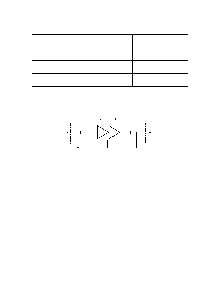
Functional Block Diagram
1
Note:
1:
Detector delivers approx. 0.5V DC into 3k
load resistor for > +18dBm output power. If output power level detection is not desired, do not make connection to
detector bond pad.
Parameter
Min
Typ
Max
Units
Frequency Range
10.5
11.7
GHz
Gate Supply Voltage
1
(Vg)
-0.5
V
Gain Small Signal (Pin = -10dBm)
18
21
dB
Gain Variation vs. Frequency
0.5
dB
Power Output Saturated: (Pin = 2dBm)
17
19
dBm
Drain Current at Psat (Pin = 2dBm)
55
mA
Power Added Efficiency (PAE): at Psat
35
%
Input Return Loss (Pin = -10dBm)
13
dB
Output Return Loss (Pin = -10dBm)
18
dB
Noise Figure
4
dB
Detector Voltage (Pout = +18dBm)
0.5
V
RF IN
RF OUT
Ground
(Back of Chip)
Drain Supply
Vd2
Drain Supply
MMIC Chip
Vd1
Output Power
Detector Voltage Vdet
Gate Supply
Vg
©2004 Fairchild Semiconductor Corporation
RMWB11001 Rev. C
RMWB11001
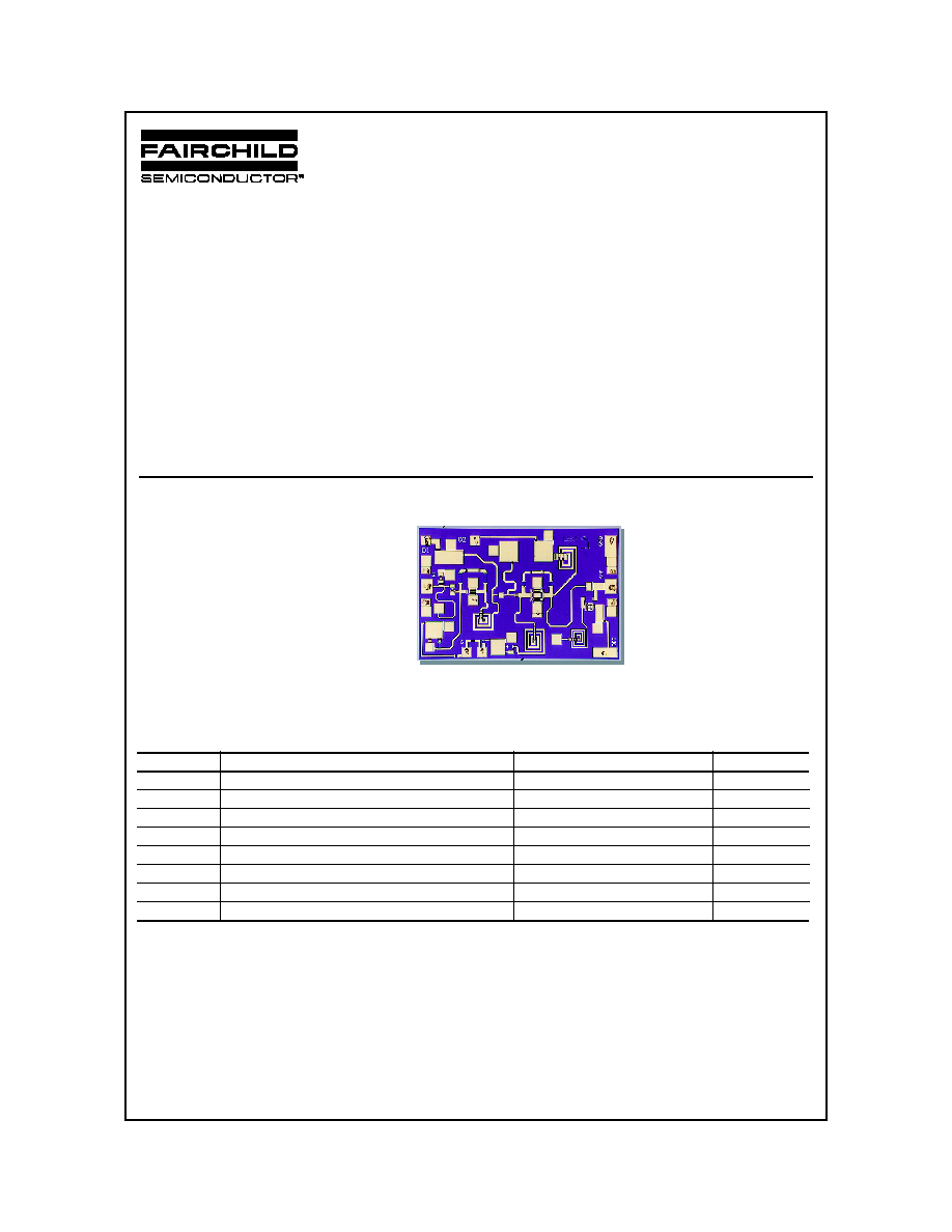
Figure 1. Chip Layout and Bond Pad Locations
Chip Size is 2.0mm x 1.3mm X 100µm. Back of chip is RF and DC Ground.
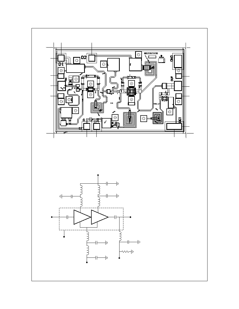
Figure 2. Recommended Application Schematic Circuit Diagram
0.5
0.11
0.577
2.0
1.3
0.0
1.3
0.65
1.828
0.106
0.0
0.0
0.0
0.567
0.720
0.873
0.567
1.145
2.0
0.873
0.720
Drain Supply
Vd=+4 V
Gate
Supply
Vg
Ground
(Back of Chip)
Output Power
Detector Voltage
Vdet
MMIC Chip
RF OUT
RF IN
100pF
100pF
10,000pF
L
L
L
L
100pF
10,000pF
L
L
L
100pF
L = Bond Wire
Inductance
3 k
Note : Detector delivers approx.
0.5V DC into 3k
load resistor
for >+18 dBm output power. If
output power level detection is
not desired, do not make
connection to detector bond
pad.
©2004 Fairchild Semiconductor Corporation
RMWB11001 Rev. C
RMWB11001
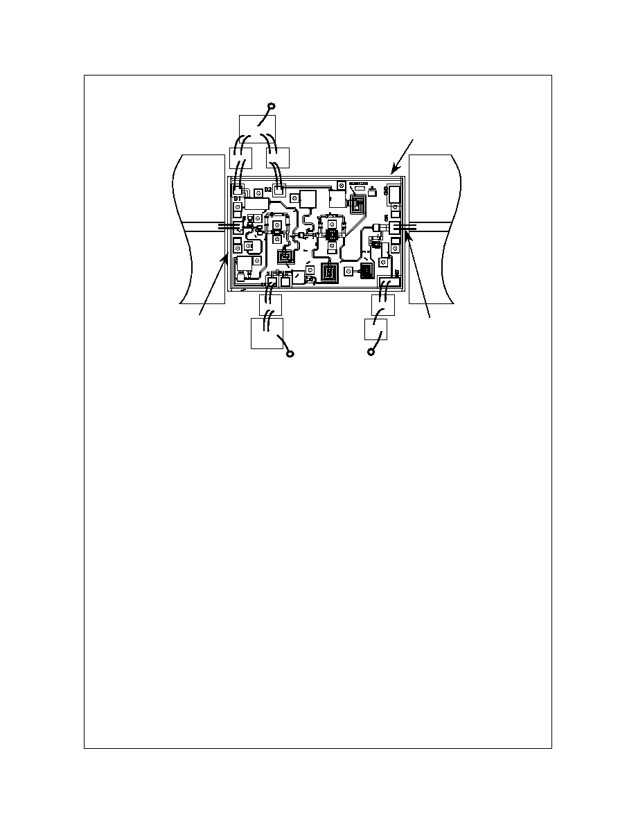
Figure 3. Recommended Assembly Diagram
Notes:
Use 0.003" by 0.0005" Gold Ribbon for bonding.RF input and output bonds should be less than 0.015" long with stress relief. Detector delivers approx. 0.5V DC into
3 k
load resistor for >+18 dBm output power. If output power level detection is not desired do not make connection to detector bond pad.
Vd
(Positive)
100pF
10,000pF
100pF
RF
Input
RF
Output
5mil Thick
Alumina
50
5 mil Thick
Alumina
50
2 mil Gap
L< 0.015"
(4 Places)
Die-Attach
80Au/20Sn
100pF
100pF
Vdet (Positive)
10,000pF
Vg (Negative)
3K
Application Information
CAUTION: THIS IS AN ESD SENSITIVE DEVICE.
Chip carrier material should be selected to have GaAs
compatible thermal coefficient of expansion and high
thermal conductivity such as copper molybdenum or copper
tungsten. The chip carrier should be machined, finished flat,
plated with gold over nickel and should be capable of
withstanding 325∞C for 15 minutes.
Die attachment should utilize Gold/Tin (80/20) eutectic alloy
solder and should avoid hydrogen environment for PHEMT
devices. Note that the backside of the chip is gold plated
and is used as RF and DC ground.
These GaAs devices should be handled with care and
stored in dry nitrogen environment to prevent contamination
of bonding surfaces. These are ESD sensitive devices and
should be handled with appropriate precaution including the
use of wrist grounding straps. All die attach and wire/ribbon
bond equipment must be well grounded to prevent static
discharges through the device.
Recommended wire bonding uses 3 mils wide and 0.5 mil
thick gold ribbon with lengths as short as practical allowing
for appropriate stress relief. The RF input and output bonds
should be typically 0.012" long corresponding to a typical 2
mil gap between the chip and the substrate material.
Recommended Procedure for Biasing and Operation
CAUTION: LOSS OF GATE VOLTAGE (Vg) WHILE
DRAIN VOLTAGE (Vd) IS PRESENT MAY DAMAGE THE
AMPLIFIER CHIP.
The following sequence of steps must be followed to
properly test the amplifier:
Step 1:
Turn off RF input power.
Step 2:
Connect the DC supply grounds to the ground of
the chip carrier. Slowly apply negative gate bias
supply voltage of -1.5V to Vg.
Step 3:
Slowly apply positive drain bias supply voltage of
+4V to Vd.
Step 4:
Adjust gate bias voltage to set the quiescent
current of Idq = 36mA.
Step 5:
After the bias condition is established, the RF input
signal may now be applied at the appropriate
frequency band.
Step 6:
Follow turn-off sequence of:
(i) Turn off RF input power,
(ii) Turn down and off drain voltage (Vd),
(iii) Turn down and off gate bias voltage (Vg).
©2004 Fairchild Semiconductor Corporation
RMWB11001 Rev. C
RMWB11001
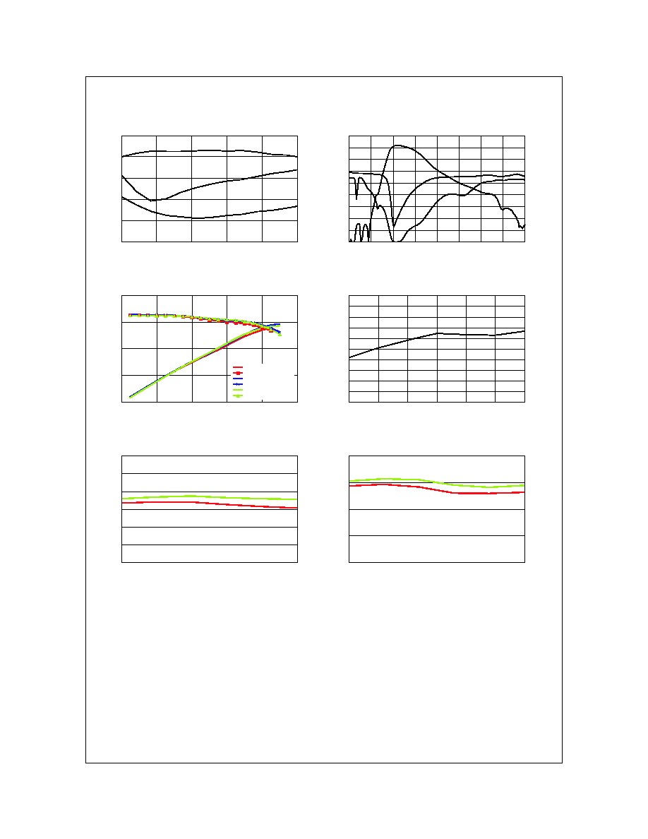
Performance Data
0
5
10
15
20
25
9.5
10
10.5
11
11.5
12
-25
-20
-15
-10
-5
0
RMWB11001, 11GHz Buffer Amplifier, Typical Performance
On-wafer Measurements, Vd=4V, Idq=36mA
S21 (dB)
Frequency (GHz)
S21
S22
S11
S11, S22 (dB)
-60
-50
-40
-30
-20
-10
0
10
20
30
0
5
10
15
20
25
30
35
40
S21 (dB)
-20
-15
-10
-5
0
5
10
S11, S22 (dB)
S21
S22
S11
Frequency (GHz)
RMWB11001, 11GHz Buffer Amplifier,
Typical Performance, Vd=4V, Idq=36mA
Chip Bonded into 50
Test Fixture
5
10
15
20
25
-16
-12
-8
-4
0
4
Input Power (dBm)
Output Power (dBm), Gain (dB)
Pout @ 10.5GHz
Gain @ 10.5GHz
Pout @ 11.1GHz
Gain @ 11.1GHz
Pout @ 11.7GHz
Gain @ 11.7GHz
RMWB11001, 11GHz Buffer Amplifier,
Typical Performance, Vd=4V, Idq=36mA
Chip Bonded into 50
Test Fixture
RMWB11001, 11GHz Buffer Amplifier,
Typical Performance, Vd=4V, Idq=36mA
Detector Voltage into 3k
load at Pout=+18dBm
10.5
10.7
10.9
11.1
11.3
11.5
11.7
Frequency (GHz)
Detector DC Voltage (V)
0
0.1
0.2
0.3
0.4
0.5
0.6
0.7
0.8
0.9
1
15
16
17
18
19
20
21
10.75
11
11.25
11.5
11.75
12
Gain at 3dB Compression (dB)
Frequency (GHz)
RMWB11001, Typical Performance Variation with Temperature,
Vd=4V, Idq=36mA, Chip Bonded into 50
Test Fixture
15
16
17
18
19
10.75
11
11.25
11.5
11.75
12
Frequency (GHz)
Output Power at 3dB Compression (dBm)
RMWB11001, Typical Performance Variation with Temperature,
Vd=4V, Idq=36mA, Chip Bonded into 50
Test Fixture