 | –≠–ª–µ–∫—Ç—Ä–æ–Ω–Ω—ã–π –∫–æ–º–ø–æ–Ω–µ–Ω—Ç: SA555 | –°–∫–∞—á–∞—Ç—å:  PDF PDF  ZIP ZIP |

©2002 Fairchild Semiconductor Corporation
www.fairchildsemi.com
www.fairchildsemi.com
www.fairchildsemi.com
www.fairchildsemi.com
Rev. 1.0.3
Features
Features
Features
Features
∑ High Current Drive Capability (200mA)
∑ Adjustable Duty Cycle
∑ Temperature Stability of 0.005%/
∞
C
∑ Timing From
µ
Sec to Hours
∑ Turn off Time Less Than 2
µ
Sec
Applications
Applications
Applications
Applications
∑ Precision Timing
∑ Pulse Generation
∑ Time Delay Generation
∑ Sequential Timing
Description
Description
Description
Description
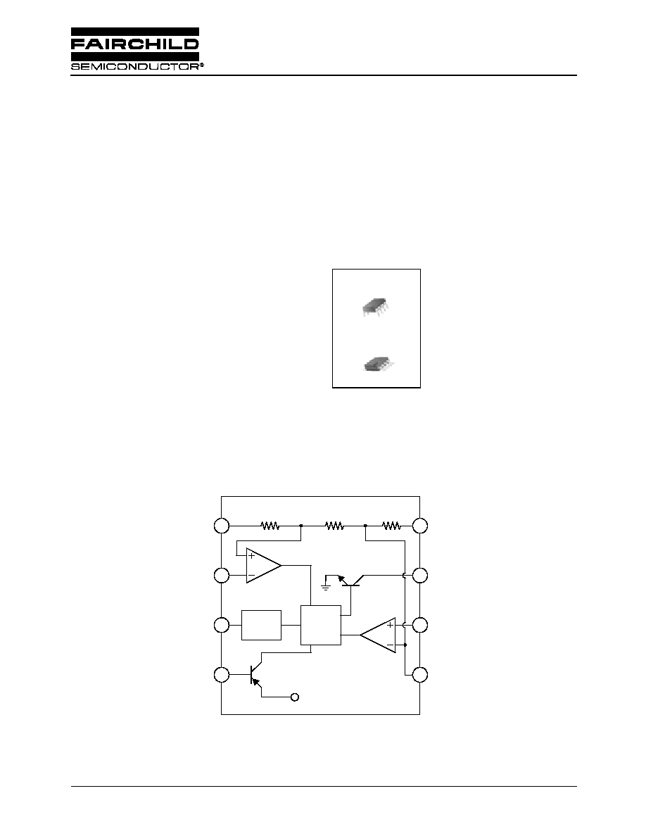
The LM555/NE555/SA555 is a highly stable controller
capable of producing accurate timing pulses. With a
monostable operation, the time delay is controlled by one
external resistor and one capacitor. With an astable
operation, the frequency and duty cycle are accurately
controlled by two external resistors and one capacitor.
8-DIP
8-DIP
8-DIP
8-DIP
8-SOP
8-SOP
8-SOP
8-SOP
1
1
Internal Block Diagram
Internal Block Diagram
Internal Block Diagram
Internal Block Diagram
F/F
F/F
F/F
F/F
OutPut
OutPut
OutPut
OutPut
Stage
Stage
Stage
Stage
1
1
1
1
7
7
7
7
5
5
5
5
2
2
2
2
3
3
3
3
4
4
4
4
6
6
6
6
8
8
8
8
R
R
R
R
R
R
R
R
R
R
R
R
Comp.
Comp.
Comp.
Comp.
Comp.
Comp.
Comp.
Comp.
Discharging Tr.
Discharging Tr.
Discharging Tr.
Discharging Tr.
Vref
Vref
Vref
Vref
Vcc
Vcc
Vcc
Vcc
Discharge
Discharge
Discharge
Discharge
Threshold
Threshold
Threshold
Threshold
Control
Control
Control
Control
Voltage
Voltage
Voltage
Voltage
GND
GND
GND
GND
Trigger
Trigger
Trigger
Trigger
Output
Output
Output
Output
Reset
Reset
Reset
Reset
LM555/NE555/SA555
Single Timer

LM555/NE555/SA555
2
2
2
2
Absolute Maximum Ratings (T
Absolute Maximum Ratings (T
Absolute Maximum Ratings (T
Absolute Maximum Ratings (T
A
A
A
A
= 25
= 25
= 25
= 25
∞
∞
∞
∞
C)
C)
C)
C)
Parameter
Parameter
Parameter
Parameter
Symbol
Symbol
Symbol
Symbol
Value
Value
Value
Value
Unit
Unit
Unit
Unit
Supply Voltage
V
CC
16
V
Lead Temperature (Soldering 10sec)
T
LEAD
300
∞
C
Power Dissipation
P
D
600
mW
Operating Temperature Range
LM555/NE555
SA555
T
OPR
0 ~ +70
-40 ~ +85
∞
C
Storage Temperature Range
T
STG
-65 ~ +150
∞
C

LM555/NE555/SA555
3
3
3
3
Electrical Characteristics
Electrical Characteristics
Electrical Characteristics
Electrical Characteristics
(T
A
= 25
∞
C, V
CC
= 5 ~ 15V, unless otherwise specified)
Notes:
Notes:
Notes:
Notes:
1. When the output is high, the supply current is typically 1mA less than at V
CC
= 5V.
2. Tested at V
CC
= 5.0V and V
CC
= 15V.
3. This will determine the maximum value of R
A
+ R
B
for 15V operation, the max. total R = 20M
, and for 5V operation, the max.
total R = 6.7M
.
4. These parameters, although guaranteed, are not 100% tested in production.
Parameter
Parameter
Parameter
Parameter
Symbol
Symbol
Symbol
Symbol
Conditions
Conditions
Conditions
Conditions
Min.
Min.
Min.
Min.
Typ.
Typ.
Typ.
Typ.
Max.
Max.
Max.
Max.
Unit
Unit
Unit
Unit
Supply Voltage
V
CC
-
4.5
-
16
V
Supply Current (Low Stable) (Note1)
I
CC
V
CC
= 5V, R
L
=
-
3
6
mA
V
CC
= 15V, R
L
=
-
7.5
15
mA
Timing Error (Monostable)
Initial Accuracy (Note2)
Drift with Temperature (Note4)
Drift with Supply Voltage (Note4)
ACCUR
t/
T
t/
V
CC
R
A
= 1k
to100k
C = 0.1
µ
F
-
1.0
50
0.1
3.0
0.5
%
ppm/
∞
C
%/V
Timing Error (Astable)
Intial Accuracy (Note2)
Drift with Temperature (Note4)
Drift with Supply Voltage (Note4)
ACCUR
t/
T
t/
V
CC
R
A
= 1k
to 100k
C = 0.1
µ
F
-
2.25
150
0.3
-
%
ppm/
∞
C
%/V
Control Voltage
V
C
V
CC
= 15V
9.0
10.0
11.0
V
V
CC
= 5V
2.6
3.33
4.0
V
Threshold Voltage
V
TH
V
CC
= 15V
-
10.0
-
V
V
CC
= 5V
-
3.33
-
V
Threshold Current (Note3)
I
TH
-
-
-
-
-
0.1
0.25
µ
A
Trigger Voltage
V
TR
V
CC
= 5V
1.1
1.67
2.2
V
V
CC
= 15V
4.5
5
5.6
V
Trigger Current
I
TR
V
TR
= 0V
0.01
2.0
µ
A
Reset Voltage
V
RST
-
-
-
-
0.4
0.7
1.0
V
Reset Current
I
RST
-
-
-
-
0.1
0.4
mA
Low Output Voltage
V
OL
V
CC
= 15V
I
SINK
= 10mA
I
SINK
= 50mA
-
0.06
0.3
0.25
0.75
V
V
V
CC
= 5V
I
SINK
= 5mA
-
0.05
0.35
V
High Output Voltage
V
OH
V
CC
= 15V
I
SOURCE
= 200mA
I
SOURCE
= 100mA
12.75
12.5
13.3
-
V
V
V
CC
= 5V
I
SOURCE
= 100mA
2.75
3.3
-
V
Rise Time of Output (Note4)
t
R
-
-
-
-
-
100
-
ns
Fall Time of Output (Note4)
t
F
-
-
-
-
-
100
-
ns
Discharge Leakage Current
I
LKG
-
-
-
-
-
20
100
nA

LM555/NE555/SA555
4
4
4
4
Application Information
Application Information
Application Information
Application Information
Table 1 below is the basic operating table of 555 timer:
When the low signal input is applied to the reset terminal, the timer output remains low regardless of the threshold voltage or
the trigger voltage. Only when the high signal is applied to the reset terminal, the timer's output changes according to
threshold voltage and trigger voltage.
When the threshold voltage exceeds 2/3 of the supply voltage while the timer output is high, the timer's internal discharge Tr.
turns on, lowering the threshold voltage to below 1/3 of the supply voltage. During this time, the timer output is maintained
low. Later, if a low signal is applied to the trigger voltage so that it becomes 1/3 of the supply voltage, the timer's internal
discharge Tr. turns off, increasing the threshold voltage and driving the timer output again at high.
1. Monostable Operation
1. Monostable Operation
1. Monostable Operation
1. Monostable Operation
Table 1. Basic Operating Table
Table 1. Basic Operating Table
Table 1. Basic Operating Table
Table 1. Basic Operating Table
Threshold Voltage
Threshold Voltage
Threshold Voltage
Threshold Voltage
(V
(V
(V
(V
th
th
th
th
)(PIN 6)
)(PIN 6)
)(PIN 6)
)(PIN 6)
Trigger Voltage
Trigger Voltage
Trigger Voltage
Trigger Voltage
(V
(V
(V
(V
tr
tr
tr
tr
)(PIN 2)
)(PIN 2)
)(PIN 2)
)(PIN 2)
Reset(PIN 4)
Reset(PIN 4)
Reset(PIN 4)
Reset(PIN 4)
Output(PIN 3)
Output(PIN 3)
Output(PIN 3)
Output(PIN 3)
Discharging Tr.
Discharging Tr.
Discharging Tr.
Discharging Tr.
(PIN 7)
(PIN 7)
(PIN 7)
(PIN 7)
Don't care
Don't care
Low
Low
ON
V
th
> 2Vcc / 3
V
th
> 2Vcc / 3
High
Low
ON
Vcc / 3 < V
th
< 2 Vcc / 3
Vcc / 3 < V
th
< 2 Vcc / 3
High
-
-
V
th
< Vcc / 3
V
th
< Vcc / 3
High
High
OFF
10
10
10
10
-5
-5
-5
-5
10
10
10
10
-4
-4
-4
-4
10
10
10
10
-3
-3
-3
-3
10
10
10
10
-2
-2
-2
-2
10
10
10
10
-1
-1
-1
-1
10
10
10
10
0
0
0
0
10
10
10
10
1
1
1
1
10
10
10
10
2
2
2
2
10
10
10
10
-3
-3
-3
-3
10
10
10
10
-2
-2
-2
-2
10
10
10
10
-1
-1
-1
-1
10
10
10
10
0
0
0
0
10
10
10
10
1
1
1
1
10
10
10
10
2
2
2
2
10M
10M
10M
10M
1M
1M
1M
1M
10k
10k
10k
10k
100
k
100
k
100
k
100
k
R
R
R
R
A
A
A
A
=1k
=1k
=1k
=1k
C
a
p
a
ci
t
a
n
ce(u
F
)
C
a
p
a
ci
t
a
n
ce(u
F
)
C
a
p
a
ci
t
a
n
ce(u
F
)
C
a
p
a
ci
t
a
n
ce(u
F
)
Time Delay(s)
Time Delay(s)
Time Delay(s)
Time Delay(s)
Figure 1. Monoatable Circuit
Figure 1. Monoatable Circuit
Figure 1. Monoatable Circuit
Figure 1. Monoatable Circuit
Figure 2. Resistance and Capacitance vs.
Figure 2. Resistance and Capacitance vs.
Figure 2. Resistance and Capacitance vs.
Figure 2. Resistance and Capacitance vs.
Time delay(t
Time delay(t
Time delay(t
Time delay(t
d
d
d
d
)
)
)
)
Figure 3. Waveforms of Monostable Operation
Figure 3. Waveforms of Monostable Operation
Figure 3. Waveforms of Monostable Operation
Figure 3. Waveforms of Monostable Operation
1
5
6
7
8
4
2
3
RESET
Vcc
DISCH
THRES
CONT
GND
OUT
TRIG
+Vcc
R
A
C1
C2
R
L
Trigger

LM555/NE555/SA555
5
5
5
5
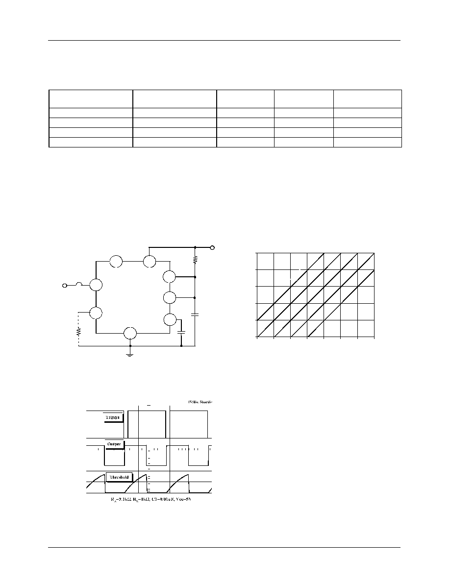
Figure 1 illustrates a monostable circuit. In this mode, the timer generates a fixed pulse whenever the trigger voltage falls
below Vcc/3. When the trigger pulse voltage applied to the #2 pin falls below Vcc/3 while the timer output is low, the timer's
internal flip-flop turns the discharging Tr. off and causes the timer output to become high by charging the external capacitor C1
and setting the flip-flop output at the same time.
The voltage across the external capacitor C1, V
C1
increases exponentially with the time constant t=R
A
*C and reaches 2Vcc/3
at td=1.1R
A
*C. Hence, capacitor C1 is charged through resistor R
A
. The greater the time constant R
A
C, the longer it takes
for the V
C1
to reach 2Vcc/3. In other words, the time constant R
A
C controls the output pulse width.
When the applied voltage to the capacitor C1 reaches 2Vcc/3, the comparator on the trigger terminal resets the flip-flop,
turning the discharging Tr. on. At this time, C1 begins to discharge and the timer output converts to low.
In this way, the timer operating in the monostable repeats the above process. Figure 2 shows the time constant relationship
based on R
A
and C. Figure 3 shows the general waveforms during the monostable operation.
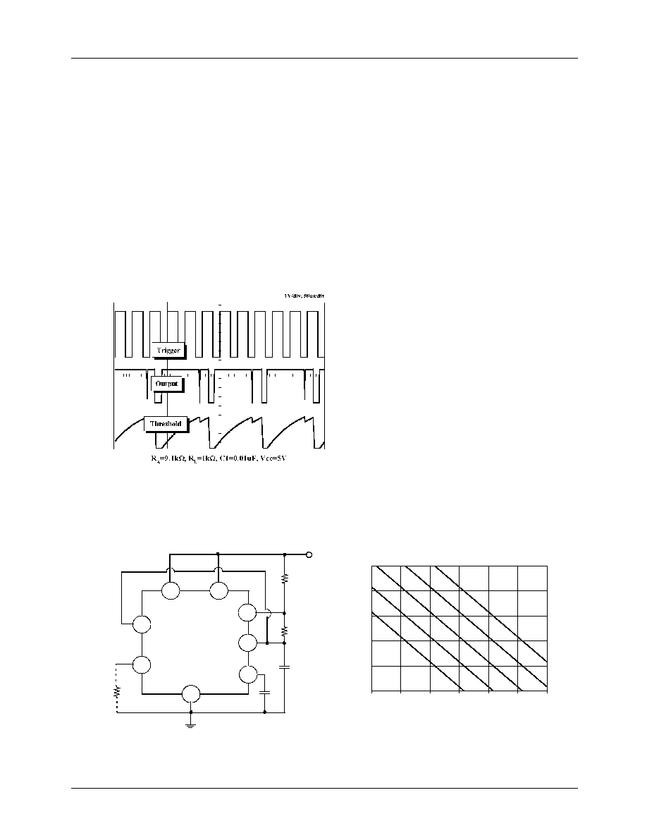
It must be noted that, for a normal operation, the trigger pulse voltage needs to maintain a minimum of Vcc/3 before the timer
output turns low. That is, although the output remains unaffected even if a different trigger pulse is applied while the output is
high, it may be affected and the waveform does not operate properly if the trigger pulse voltage at the end of the output pulse
remains at below Vcc/3. Figure 4 shows such a timer output abnormality.
2. Astable Operation
2. Astable Operation
2. Astable Operation
2. Astable Operation
Figure 4. Waveforms of Monostable Operation (abnormal)
Figure 4. Waveforms of Monostable Operation (abnormal)
Figure 4. Waveforms of Monostable Operation (abnormal)
Figure 4. Waveforms of Monostable Operation (abnormal)
100m
100m
100m
100m
1
1
1
1
10
10
10
10
100
100
100
100
1k
1k
1k
1k
10k
10k
10k
10k
100k
100k
100k
100k
1E-3
1E-3
1E-3
1E-3
0.01
0.01
0.01
0.01
0.1
0.1
0.1
0.1
1
1
1
1
10
10
10
10
100
100
100
100
10M
10M
10M
10M
1M
1M
1M
1M
100k
100k
100k
100k
10k
10k
10k
10k
1k
1k
1k
1k
(R
(R
(R
(R
A
A
A
A
+2R
+2R
+2R
+2R
B
B
B
B
)
)
)
)
C
a
p
a
cit
a
n
ce(u
F
)
C
a
p
a
cit
a
n
ce(u
F
)
C
a
p
a
cit
a
n
ce(u
F
)
C
a
p
a
cit
a
n
ce(u
F
)
Fr equency(Hz)
Fr equency(Hz)
Fr equency(Hz)
Fr equency(Hz)
Figure 5. Astable Circuit
Figure 5. Astable Circuit
Figure 5. Astable Circuit
Figure 5. Astable Circuit
Figure 6. Capacitance and Resistance vs. Frequency
Figure 6. Capacitance and Resistance vs. Frequency
Figure 6. Capacitance and Resistance vs. Frequency
Figure 6. Capacitance and Resistance vs. Frequency
1
5
6
7
8
4
2
3
RESET
Vcc
DISCH
THRES
CONT
GND
OUT
TRIG
+Vcc
R
A
C1
C2
R
L
R
B

LM555/NE555/SA555
6
6
6
6
An astable timer operation is achieved by adding resistor R
B
to Figure 1 and configuring as shown on Figure 5. In the astable
operation, the trigger terminal and the threshold terminal are connected so that a self-trigger is formed, operating as a multi
vibrator. When the timer output is high, its internal discharging Tr. turns off and the V
C1
increases by exponential
function with the time constant (R
A
+R
B
)*C.
When the V
C1
, or the threshold voltage, reaches 2Vcc/3, the comparator output on the trigger terminal becomes high,
resetting the F/F and causing the timer output to become low. This in turn turns on the discharging Tr. and the C1 discharges
through the discharging channel formed by R
B
and the discharging Tr. When the V
C1
falls below Vcc/3, the comparator
output on the trigger terminal becomes high and the timer output becomes high again. The discharging Tr. turns off and the
V
C1
rises again.
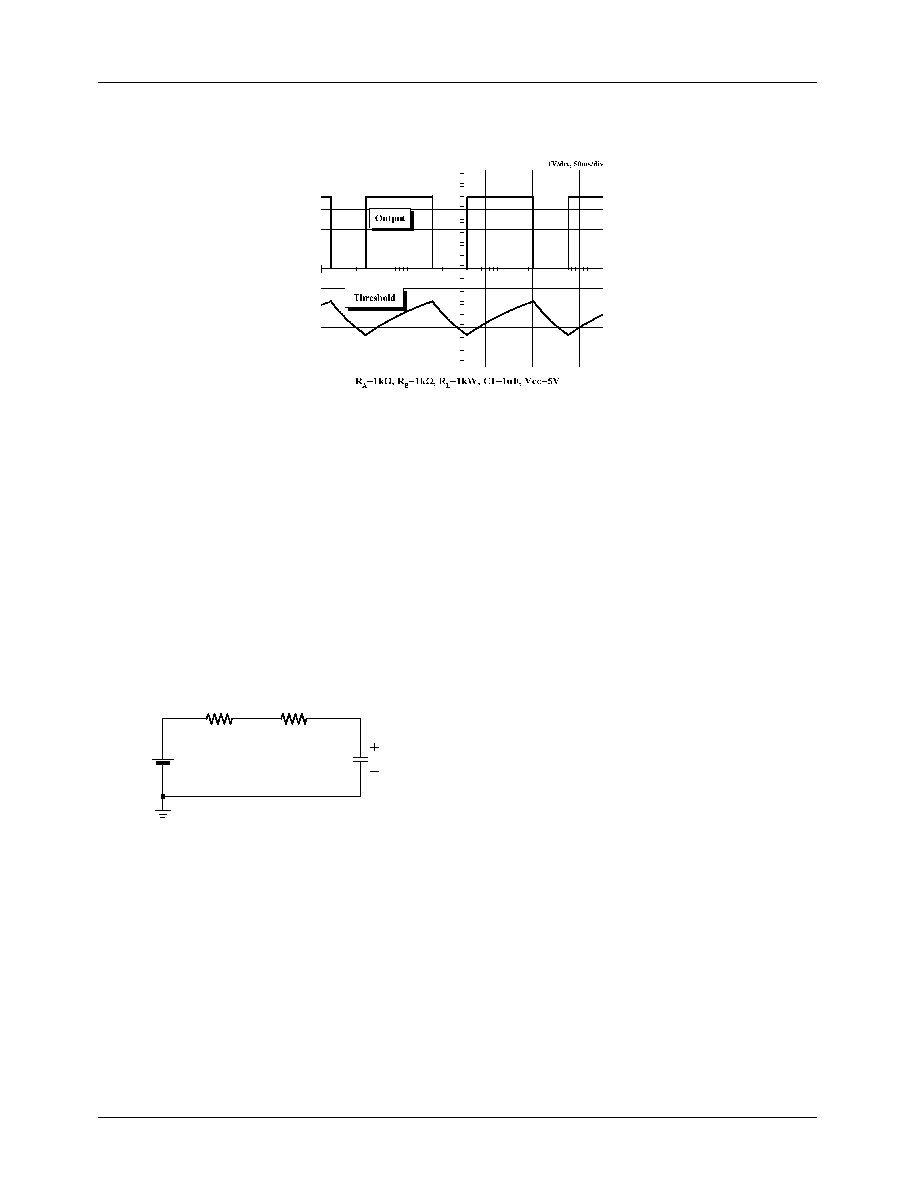
In the above process, the section where the timer output is high is the time it takes for the V
C1
to rise from Vcc/3 to 2Vcc/3,
and the section where the timer output is low is the time it takes for the V
C1
to drop from 2Vcc/3 to Vcc/3. When timer output
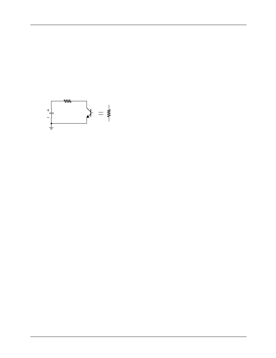
is high, the equivalent circuit for charging capacitor C1 is as follows:
Since the duration of the timer output high state(t
H
) is the amount of time it takes for the V
C1
(t) to reach 2Vcc/3,
Figure 7. Waveforms of Astable Operation
Figure 7. Waveforms of Astable Operation
Figure 7. Waveforms of Astable Operation
Figure 7. Waveforms of Astable Operation
Vcc
R
A
R
B
C1
Vc1(0-)=Vcc/3
C1
dvc1
dt
-------------
Vcc V 0-
( )
≠
RA RB
+
-------------------------------
=
1
( )
VC1 0+
(
)
VCC 3
/
=
2
( )
VC1 t
( )
VCC 1
2
3
---
e
-
t
RA RB
+
(
)
C1
------------------------------------
≠
≠
=
3
( )

LM555/NE555/SA555
7
7
7
7
The equivalent circuit for discharging capacitor C1, when timer output is low is, as follows:
Since the duration of the timer output low state(
t
L
) is the amount of time it takes for the V
C1
(t) to reach Vcc/3,
Since R
D
is normally R
B
>>R
D
although related to the size of discharging Tr.,
t
L
=0.693R
B
C
1
(10)
Consequently, if the timer operates in astable, the period is the same with
'T=t
H
+t
L
=0.693(RA+R
B
)C
1
+0.693R
B
C
1
=0.693(R
A
+2R
B
)C
1
' because the period is the sum of the charge time and discharge
time. And since frequency is the reciprocal of the period, the following applies.
3. Frequency divider
3. Frequency divider
3. Frequency divider
3. Frequency divider
By adjusting the length of the timing cycle, the basic circuit of Figure 1 can be made to operate as a frequency divider. Figure
8. illustrates a divide-by-three circuit that makes use of the fact that retriggering cannot occur during the timing cycle.
VC1 t
( )
2
3
---
VCC V
=
CC
1
2
3
---
e
-
tH
RA RB
+
(
)
C1
------------------------------------
≠
≠
=
4
( )
tH C1 RA RB
+
(
)
In2
0.693 RA RB
+
(
)
C1
=
=
5
( )
C1
R
B
R
D
V
C1
(0-)=2Vcc/3
C1
dvC1
dt
--------------
1
RA RB
+
-----------------------
VC1 0
=
+
6
( )
VC1 t
( )
2
3
---
V
CC
e
-
t
RA RD
+
(
)
C1
-------------------------------------
=
7
( )
1
3
---
VCC
2
3
---
V
CC
e
-
tL
RA RD
+
(
)
C1
-------------------------------------
=
8
( )
tL C1 RB RD
+
(
)
In2
0.693 RB RD
+
(
)
C1
=
=
9
( )
frequency,
f
1
T
---
1.44
RA 2RB
+
(
)
C1
----------------------------------------
=
=
11
( )

LM555/NE555/SA555
8
8
8
8
4. Pulse Width Modulation
4. Pulse Width Modulation
4. Pulse Width Modulation
4. Pulse Width Modulation
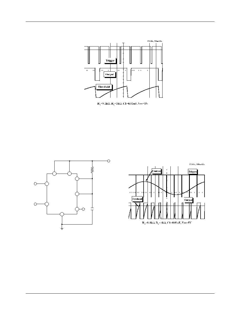
The timer output waveform may be changed by modulating the control voltage applied to the timer's pin 5 and changing the
reference of the timer's internal comparators. Figure 9 illustrates the pulse width modulation circuit.
When the continuous trigger pulse train is applied in the monostable mode, the timer output width is modulated according to
the signal applied to the control terminal. Sine wave as well as other waveforms may be applied as a signal to the control
terminal. Figure 10 shows the example of pulse width modulation waveform.
5. Pulse Position Modulation
5. Pulse Position Modulation
5. Pulse Position Modulation
5. Pulse Position Modulation
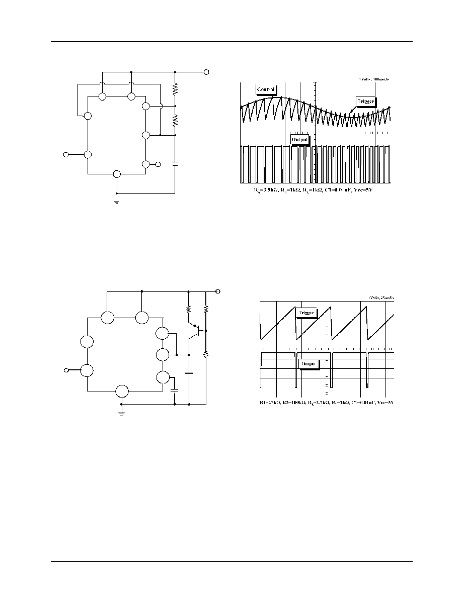
If the modulating signal is applied to the control terminal while the timer is connected for the astable operation as in Figure 11,
the timer becomes a pulse position modulator.
In the pulse position modulator, the reference of the timer's internal comparators is modulated which in turn modulates the
timer output according to the modulation signal applied to the control terminal.
Figure 12 illustrates a sine wave for modulation signal and the resulting output pulse position modulation : however, any wave
shape could be used.
Figure 8. Waveforms of Frequency Divider Operation
Figure 8. Waveforms of Frequency Divider Operation
Figure 8. Waveforms of Frequency Divider Operation
Figure 8. Waveforms of Frequency Divider Operation
Figure 9. Circuit for Pulse Width Modulation
Figure 9. Circuit for Pulse Width Modulation
Figure 9. Circuit for Pulse Width Modulation
Figure 9. Circuit for Pulse Width Modulation
Figure 10. Waveforms of Pulse Width Modulation
Figure 10. Waveforms of Pulse Width Modulation
Figure 10. Waveforms of Pulse Width Modulation
Figure 10. Waveforms of Pulse Width Modulation
8
4
7
1
2
3
5
6
CONT
GND
Vcc
DISCH
THRES
RESET
TRIG
OUT
+Vcc
+Vcc
+Vcc
+Vcc
Trigger
Trigger
Trigger
Trigger
R
R
R
R
A
A
A
A
C
C
C
C
Output
Output
Output
Output
Input
Input
Input
Input

LM555/NE555/SA555
9
9
9
9
6. Linear Ramp
6. Linear Ramp
6. Linear Ramp
6. Linear Ramp
When the pull-up resistor RA in the monostable circuit shown in Figure 1 is replaced with constant current source, the V
C1
increases linearly, generating a linear ramp. Figure 13 shows the linear ramp generating circuit and Figure 14 illustrates the
generated linear ramp waveforms.
In Figure 13, current source is created by PNP transistor Q1 and resistor R1, R2, and R
E
.
For example, if Vcc=15V, R
E
=20k
, R1=5kW, R2=10k
, and V
BE
=0.7V,
V
E
=0.7V+10V=10.7V
Ic=(15-10.7)/20k=0.215mA
8
4
7
1
2
3
5
6
CONT
GND
Vcc
DISCH
THRES
RESET
TRIG
OUT
+Vcc
+Vcc
+Vcc
+Vcc
R
R
R
R
A
A
A
A
C
C
C
C
R
R
R
R
B
B
B
B
Modulation
Modulation
Modulation
Modulation
Output
Output
Output
Output
Figure 11. Circuit for Pulse Position Modulation
Figure 11. Circuit for Pulse Position Modulation
Figure 11. Circuit for Pulse Position Modulation
Figure 11. Circuit for Pulse Position Modulation
Figure 12. Waveforms of pulse position modulation
Figure 12. Waveforms of pulse position modulation
Figure 12. Waveforms of pulse position modulation
Figure 12. Waveforms of pulse position modulation
Figure 13. Circuit for Linear Ramp
Figure 13. Circuit for Linear Ramp
Figure 13. Circuit for Linear Ramp
Figure 13. Circuit for Linear Ramp
Figure 14. Waveforms of Linear Ramp
Figure 14. Waveforms of Linear Ramp
Figure 14. Waveforms of Linear Ramp
Figure 14. Waveforms of Linear Ramp
1
5
6
7
8
4
2
3
RESET
Vcc
DISCH
THRES
CONT
GND
OUT
TRIG
+Vcc
C2
R1
R2
C1
Q1
Output
R
E
IC
VCC VE
≠
RE
---------------------------
=
12
( )
Here, VE is
VE VBE
R2
R1 R2
+
----------------------
VCC
+
=
13
( )

LM555/NE555/SA555
10
10
10
10
When the trigger starts in a timer configured as shown in Figure 13, the current flowing through capacitor C1 becomes a
constant current generated by PNP transistor and resistors.
Hence, the V
C
is a linear ramp function as shown in Figure 14. The gradient S of the linear ramp function is defined as
follows:
Here the Vp-p is the peak-to-peak voltage.
If the electric charge amount accumulated in the capacitor is divided by the capacitance, the V
C
comes out as follows:
V=Q/C
(15)
The above equation divided on both sides by T gives us
and may be simplified into the following equation.
S=I/C
(17)
In other words, the gradient of the linear ramp function appearing across the capacitor can be obtained by using the constant
current flowing through the capacitor.
If the constant current flow through the capacitor is 0.215mA and the capacitance is 0.02
µ
F, the gradient of the ramp function
at both ends of the capacitor is S = 0.215m/0.022
µ
= 9.77V/ms.
S
Vp p
≠
T
----------------
=
14
( )
V
T
----
Q T
/
C
------------
=
16
( )

LM555/NE555/SA555
11
11
11
11
Mechanical Dimensions
Mechanical Dimensions
Mechanical Dimensions
Mechanical Dimensions
Package
Package
Package
Package
Dimensions in millimeters
Dimensions in millimeters
Dimensions in millimeters
Dimensions in millimeters
6.40
±
0.20
3.30
±
0.30
0.130
±
0.012
3.40
±
0.20
0.134
±
0.008
#1
#4
#5
#8
0.252
±
0.008
9.20
±
0.20
0.79
2.54
0.100
0.031
()
0.46
±
0.10
0.018
±
0.004
0.060
±
0.004
1.524
±
0.10
0.362
±
0.008
9.60
0.378
MAX
5.08
0.200
0.33
0.013
7.62
0~15
∞
0.300
MAX
MIN
0.25
+0.10
≠0.05
0.010
+0.004
≠0.002
8-DIP
8-DIP
8-DIP
8-DIP

LM555/NE555/SA555
12
12
12
12
Mechanical Dimensions
Mechanical Dimensions
Mechanical Dimensions
Mechanical Dimensions
(Continued)
Package
Package
Package
Package
Dimensions in millimeters
Dimensions in millimeters
Dimensions in millimeters
Dimensions in millimeters
4.92
±
0.20
0.194
±
0.008
0.41
±
0.10
0.016
±
0.004
1.27
0.050
5.72
0.225
1.55
±
0.20
0.061
±
0.008
0.1~0.25
0.004~0.001
6.00
±
0.30
0.236
±
0.012
3.95
±
0.20
0.156
±
0.008
0.50
±
0.20
0.020
±
0.008
5.13
0.202
MAX
#1
#4
#5
0~8
∞
#8
0.56
0.022
()
1.80
0.071
MAX0.10
MAX0.004
MAX
MIN
+
0.10
-0.05
0.15
+
0.004
-0.002
0.006
8-SOP
8-SOP
8-SOP
8-SOP

LM555/NE555/SA555
13
13
13
13
Ordering Information
Ordering Information
Ordering Information
Ordering Information
Product Number
Product Number
Product Number
Product Number
Package
Package
Package
Package
Operating Temperature
Operating Temperature
Operating Temperature
Operating Temperature
LM555CN
8-DIP
0 ~ +70
∞
C
LM555CM
8-SOP
Product Number
Product Number
Product Number
Product Number
Package
Package
Package
Package
Operating Temperature
Operating Temperature
Operating Temperature
Operating Temperature
NE555N
8-DIP
0 ~ +70
∞
C
NE555D
8-SOP
Product Number
Product Number
Product Number
Product Number
Package
Package
Package
Package
Operating Temperature
Operating Temperature
Operating Temperature
Operating Temperature
SA555
8-DIP
-40 ~ +85
∞
C
SA555D
8-SOP

LM555/NE555/SA555
LM555/NE555/SA555
LM555/NE555/SA555
LM555/NE555/SA555
11/29/02 0.0m 001
Stock#DSxxxxxxxx
2002 Fairchild Semiconductor Corporation
LIFE SUPPORT POLICY
LIFE SUPPORT POLICY
LIFE SUPPORT POLICY
LIFE SUPPORT POLICY
FAIRCHILD'S PRODUCTS ARE NOT AUTHORIZED FOR USE AS CRITICAL COMPONENTS IN LIFE SUPPORT DEVICES
OR SYSTEMS WITHOUT THE EXPRESS WRITTEN APPROVAL OF THE PRESIDENT OF FAIRCHILD SEMICONDUCTOR
CORPORATION. As used herein:
1. Life support devices or systems are devices or systems
which, (a) are intended for surgical implant into the body,
or (b) support or sustain life, and (c) whose failure to
perform when properly used in accordance with
instructions for use provided in the labeling, can be
reasonably expected to result in a significant injury of the
user.
2. A critical component in any component of a life support
device or system whose failure to perform can be
reasonably expected to cause the failure of the life support
device or system, or to affect its safety or effectiveness.
www.fairchildsemi.com
DISCLAIMER
DISCLAIMER
DISCLAIMER
DISCLAIMER
FAIRCHILD SEMICONDUCTOR RESERVES THE RIGHT TO MAKE CHANGES WITHOUT FURTHER NOTICE TO ANY
PRODUCTS HEREIN TO IMPROVE RELIABILITY, FUNCTION OR DESIGN. FAIRCHILD DOES NOT ASSUME ANY
LIABILITY ARISING OUT OF THE APPLICATION OR USE OF ANY PRODUCT OR CIRCUIT DESCRIBED HEREIN; NEITHER
DOES IT CONVEY ANY LICENSE UNDER ITS PATENT RIGHTS, NOR THE RIGHTS OF OTHERS.
