 | –≠–ª–µ–∫—Ç—Ä–æ–Ω–Ω—ã–π –∫–æ–º–ø–æ–Ω–µ–Ω—Ç: SB580 | –°–∫–∞—á–∞—Ç—å:  PDF PDF  ZIP ZIP |

FMB100
FMB100
NPN Multi-Chip General Purpose Amplifier
This device is designed for general purpose amplifier applications at collector
currents to 300 mA. Sourced from Process 10.
Absolute Maximum Ratings*
T
A
=25∞C unless otherwise noted
*
These ratings are limiting values above which the serviceability of any semiconductor device may be impaired.
NOTES:
1) These ratings are based on a maximum junction temperature of 150 degrees C.
2) These are steady state limits. The factory should be consulted on applications involving pulsed or low duty cycle operations.
Discrete POWER & Signal
Technologies
Symbol
Parameter
Value
Units
V
CEO
Collector-Emitter Voltage
45
V
V
CBO
Collector-Base Voltage
75
V
V
EBO
Emitter-Base Voltage
6.0
V
I
C
Collector Current - Continuous
500
mA
T
J
, T
stg
Operating and Storage Junction Temperature Range
-55 to +150
∞
C
Thermal Characteristics
T
A
= 25∞C unless otherwise noted
Symbol
Characteristic
Max
Units
FMB100
P
D
Total Device Dissipation
Derate above 25
∞
C
700
5.6
mW
mW/
∞
C
R
JA
Thermal Resistance, Junction to Ambient
180
∞
C/W
©
1998 Fairchild Semiconductor Corporation
SuperSOT
TM
-6
Mark: .NA
C1
E1
C2
B1
E2
B2
pin #1

FMB100
NPN Multi-Chip General Purpose Amplifier
(continued)
Electrical Characteristics
T
A
= 25∞C unless otherwise noted
OFF CHARACTERISTICS
ON CHARACTERISTICS
SMALL SIGNAL CHARACTERISTICS
*
Pulse Test: Pulse Width
300
µ
s, Duty Cycle
2.0%
BV
CBO
Collector-Base Breakdown Voltage
I
C
= 10
µ
A, I
B
= 0
75
V
BV
CEO
Collector-Emitter Breakdown
Voltage*
I
C
= 1 mA, I
E
= 0
45
V
BV
EBO
Emitter-Base Breakdown Voltage
I
E
= 10
µ
A, I
C
= 0
6.0
V
I
CBO
Collector Cutoff Current
V
CB
= 60 V
50
nA
I
CES
Collector Cutoff Current
V
CE
= 40 V
50
nA
I
EBO
Emitter Cutoff Current
V
EB
= 4 V
50
nA
h
FE
DC Current Gain
I
C
= 100
µ
A, V
CE
= 1.0 V
I
C
= 10 mA, V
CE
= 1.0 V
I
C
= 100 mA, V
CE
= 1.0 V*
I
C
= 150 mA, V
CE
= 5.0 V*
80
100
100
100
450
350
V
CE(
sat
)
Collector-Emitter Saturation Voltage
I
C
= 10 mA, I
B
= 1.0 mA
I
C
= 200 mA, I
B
= 20 mA*
0.2
0.4
V
V
V
BE(
sat
)
Base-Emitter Saturation Voltage
I
C
= 10 mA, I
B
= 1.0 mA
I
C
= 200 mA, I
B
= 20 mA*
0.85
1.0
V
V
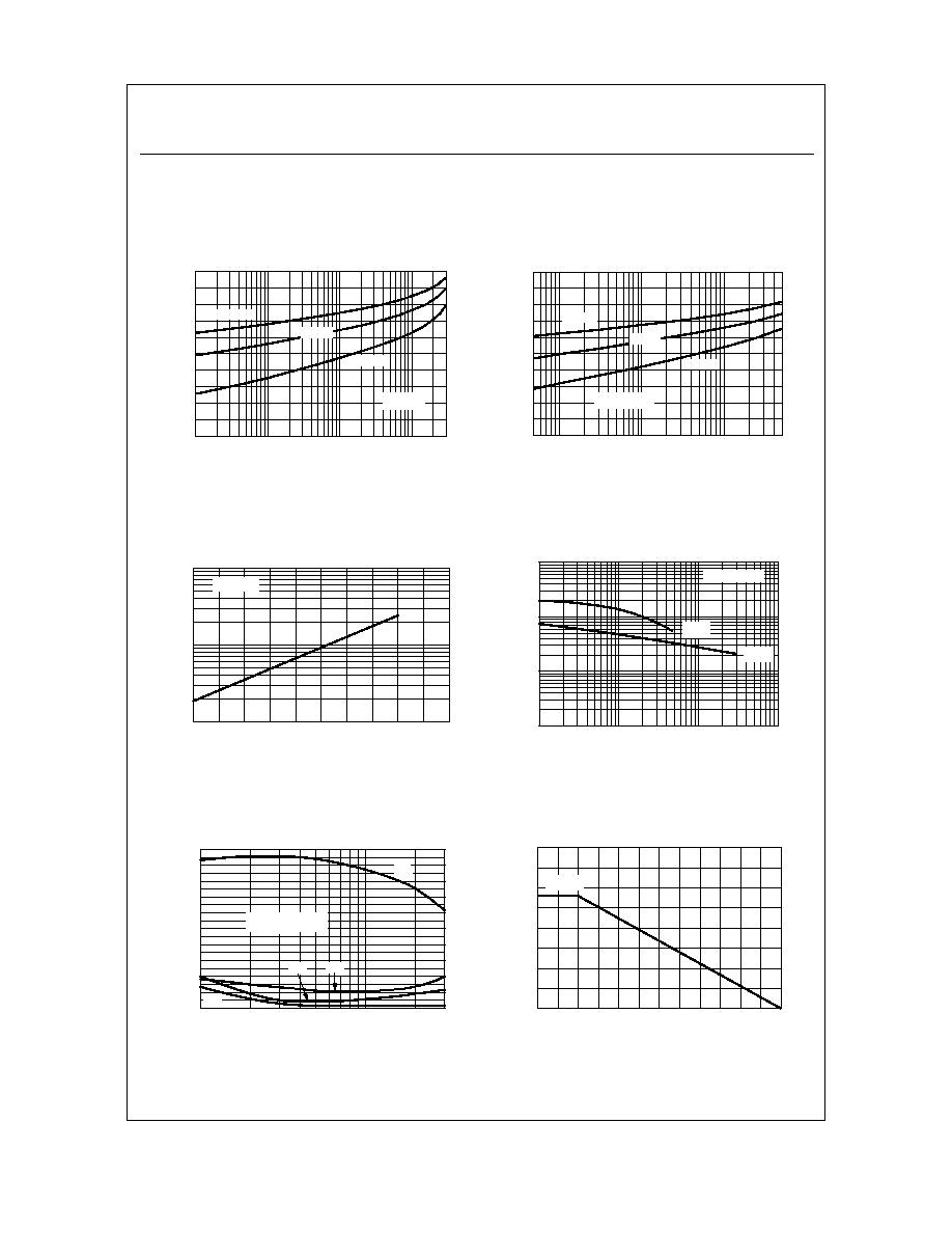
Typical Characteristics
Typical Pulsed Current Gain
vs Collector Current
10
20
30
50
100
200 300
500
0
100
200
300
400
I - COLLECTOR CURRENT (mA)
h
- TYP
ICA
L PULSED
CURR
ENT GA
IN
C
FE
125 ∞C
25 ∞C
- 40 ∞C
Vce = 5V
Collector-Emitter Saturation
Voltage vs Collector Current
1
10
100
400
0.1
0.2
0.3
0.4
I - COLLECTOR CURRENT (mA)
V - COLLE
CT
O
R
-E
M
I
T
TER VOL
T
A
GE (V)
C
C
ESA
T
25 ∞C
- 40 ∞C
125 ∞C
= 10
f
T
Current Gain - Bandwidth Product
V
CE
= 20 V, I
C
= 20 mA
300
MHz
C
obo
Output Capacitance
V
CB
= 5.0 V, f = 1.0 MHz
3.5
pF
NF
Noise Figure
I
C
= 100
µ
A, V
CE
= 5.0 V,
R
G
= 2.0 k
, f = 1.0 kHz
2.5
dB
Symbol
Parameter
Test Conditions
Min
Typ
Max Units
FMB100
Typical Characteristics
(continued)
NPN Multi-Chip General Purpose Amplifier
(continued)
Base-Emitter Saturation
Voltage vs Collector Current
0.1
1
10
100
300
0.2
0.4
0.6
0.8
1
I - COLLECTOR CURRENT (mA)
V
-
CO
LLE
CTOR
-
E
M
I
TT
ER
V
O
L
T
A
G
E
(
V
)
= 10
C
B
ESA
T
25 ∞C
- 40 ∞C
125 ∞C
Base-Emitter ON Voltage vs
Collector Current
1
10
100
500
0.2
0.4
0.6
0.8
1
I - COLLECTOR CURRENT (mA)
V
-
BA
SE
-
E
MITTER
ON VO
L
T
A
GE (V
)
C
BE
O
N
V = 5V
CE
25 ∞C
- 40 ∞C
125 ∞C
Collector-Cutoff Current
vs Ambient Temperature
25
50
75
100
125
150
0.1
1
10
T - AMBIENT TEMPERATURE ( C)
I
- CO
LLE
CT
O
R
CURR
EN
T
(
n
A
)
A
CBO
V = 60V
∫
CB
Input and Output Capacitance
vs Reverse Voltage
0.1
1
10
100
0.1
1
10
100
V - COLLECTOR VOLTAGE(V)
CA
P
A
CIT
A
NCE
(
pF)
Cib
Cob
f = 1.0 MHz
ce
Switching Times vs
Collector Current
10
20
30
50
100
200
300
0
30
60
90
120
150
180
210
240
270
300
I - COLLECTOR CURRENT (mA)
T
I
ME
(n
S
)
IB1 = IB2 = Ic / 10
V = 10 V
C
cc
t
s
t
d
t
f
t
r
Power Dissipation vs
Ambient Temperature
0
25
50
75
100
125
150
0
0.25
0.5
0.75
1
TEMPERATURE ( C)
P
-
P
O
WER DISSIP
A
T
I
O
N
(
W
)
D
o
SOT-6