 | –≠–ª–µ–∫—Ç—Ä–æ–Ω–Ω—ã–π –∫–æ–º–ø–æ–Ω–µ–Ω—Ç: SPT5230 | –°–∫–∞—á–∞—Ç—å:  PDF PDF  ZIP ZIP |
Document Outline
- Main Menu
- Selection Guide
- Data Conversion
- Analog to Digital
- Search
- fairchildsemi.com
SPT5230
10-BIT, 36 MWPS TRIPLE VIDEO DAC
Current
Switch
Cell
Array
(Cell 4)
Current
Switch Cell
Array (Cell 255)
Latch
Decoder
Latch
R
OUT
CLKR
V
CS
V
REF
Current
Switch Cell
Array (Cell 255)
Latch
Decoder
Latch
B
OUT
CLKB
Latch
Decoder
Latch
Current
Switch Cell
Array (Cell 255)
G
OUT
CLKG
AV
DD
I
OR
I
OB
VSSA
I
OG
(LSB) DRÿ
DR1
DR2
DR3
DR4
DR5
DR6
DR7
(MSB) DR9
DR8
(LSB) DGÿ
DG1
DG2
DG3
DG4
DG5
DG6
DG7
(MSB) DG9
DG8
(LSB) DBÿ
DB1
DB2
DB3
DB4
DB5
DB6
DB7
(MSB) DB9
DB8
V
REF1
Current
Switch
Cell
Array
(Cell 4)
Current
Switch
Cell
Array
(Cell 4)
V
REF2
V
CS2
V
CS1
AV
DD
AV
DD
AV
DD
FEATURES
∑ 10-Bit Triple Video Digital-to-Analog Converter
∑ Output Full-Scale Voltage 0.5 to 2.0 Vp-p
∑ 36 MWPS Operation (typ)
∑ Low Power: 280 mW (1 Vp-p Output)
∑ 5 V Monolithic CMOS
∑ 52-pin QFP Package (10mm x 10mm, 0.65 mm pitch)
APPLICATIONS
∑ Desktop Video Processing
∑ CCIR-601 Video Signal Processing
∑ RGB Color Monitors
∑ Image Processing
∑ Direct Digital Synthesis
the full-scale output current. The differential linearity errors of
the DACs are guaranteed to be a maximum of
±
1.0 LSB over
the full temperature range. The device is available in a 52-
lead QFP package over the commercial temperature range.
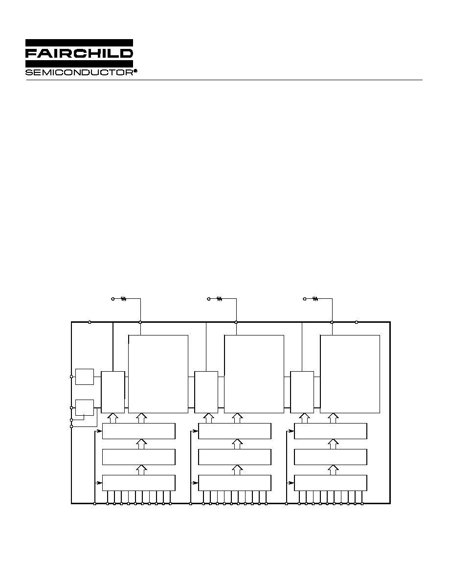
GENERAL DESCRIPTION
The SPT5230 is a 10-bit, 36 MWPS triple video digital-to-
analog converter specifically designed for high performance,
high resolution color graphics monitor applications and video
processing applications. A single external resistor controls
BLOCK DIAGRAM

2
5 / 1 / 0 0
SPT5230
Note: 1. Operation at any Absolute Maximum Rating is not implied. See Electrical Specifications for proper nominal applied
conditions in typical applications.
ABSOLUTE MAXIMUM RATINGS (Beyond which damage may occur)
1
Supply Voltages
AV
DD
(measured to AV
SS
) ........................... ≠0.3 to 7.0 V
Input Voltage
Clock and Data ......................................... AV
SS
to AV
DD
Output Current
I
OUT ...........................................................................
0 to 14 mA
Temperature
Operating, ambient ........................................ 0 to +70
∞
C
Storage ................................................... ≠55 to + 125
∞
C
ELECTRICAL SPECIFICATIONS
f
CLK
= 27 MWPS, AV
DD
= 5.0 V, Output Pull-Up Load = 75
, T
A
= 25
∞
C, AV
SS
= 0.0 V
TEST
TEST
PARAMETERS
CONDITIONS
LEVEL
MIN
TYP
MAX
UNITS
DC Performance
Resolution
10.0
Bits
Differential Linearity
T
A
= T
MIN
to T
MAX
I
≠1.0
1.0
LSB
Integral Linearity
I
≠2.5
2.0
LSB
Analog Outputs
Output Voltage Range
V
CS2
= +2.1 V
I
3.0
5.0
V
Conversion Rate
I
27
36
MWPS
Output Offset Voltage
I
2.4
14
mV
Signal-to-Noise Ratio
I
46
52
dB
Settling Time
1
I
16
23
ns
Propagation Delay (t
pd
)
V
10
12
ns
Crosstalk
I
≠49
≠54
dB
FS Control Voltage (V
CS2
)
V
2.0
4.0
V
Digital Inputs and Timing
Input Current, Logic High
V
IH
= 5 V
I
5
µ
A
Logic Low
V
IL
= 0 V
I
≠5
µ
A
Set-Up Time, Data and Controls (t
S
)
I
5
ns
Hold Time, Data and Controls (t
h
)
I
10
ns
Clock Duty Cycle
V
40
60
%
Power Supply Requirements
Supply Voltage
I
4.75
5.25
V
Supply Current
1 Vp-p Output
IV
56
mA
2 Vp-p Output
I
100
mA
Power Dissipation
1 Vp-p Output
IV
280
mW
2 Vp-p Output
I
485
500
mW
1
Full-scale settling time to within
±
2% of full scale.
TEST LEVEL CODES
All electrical characteristics are subject to the
following conditions:
All parameters having min/max specifications
are guaranteed. The Test Level column indi-
cates the specific device testing actually per-
formed during production and Quality Assur-
ance inspection. Any blank section in the data
column indicates that the specification is not
tested at the specified condition.
TEST PROCEDURE
100% production tested at the specified temperature.
100% production tested at T
A
=25
∞
C, and sample
tested at the specified temperatures.
QA sample tested only at the specified temperatures.
Parameter is guaranteed (but not tested) by design
and characterization data.
Parameter is a typical value for information purposes
only.
100% production tested at T
A
= 25
∞
C. Parameter is
guaranteed over specified temperature range.
TEST LEVEL
I
II
III
IV
V
VI

3
5 / 1 / 0 0
SPT5230
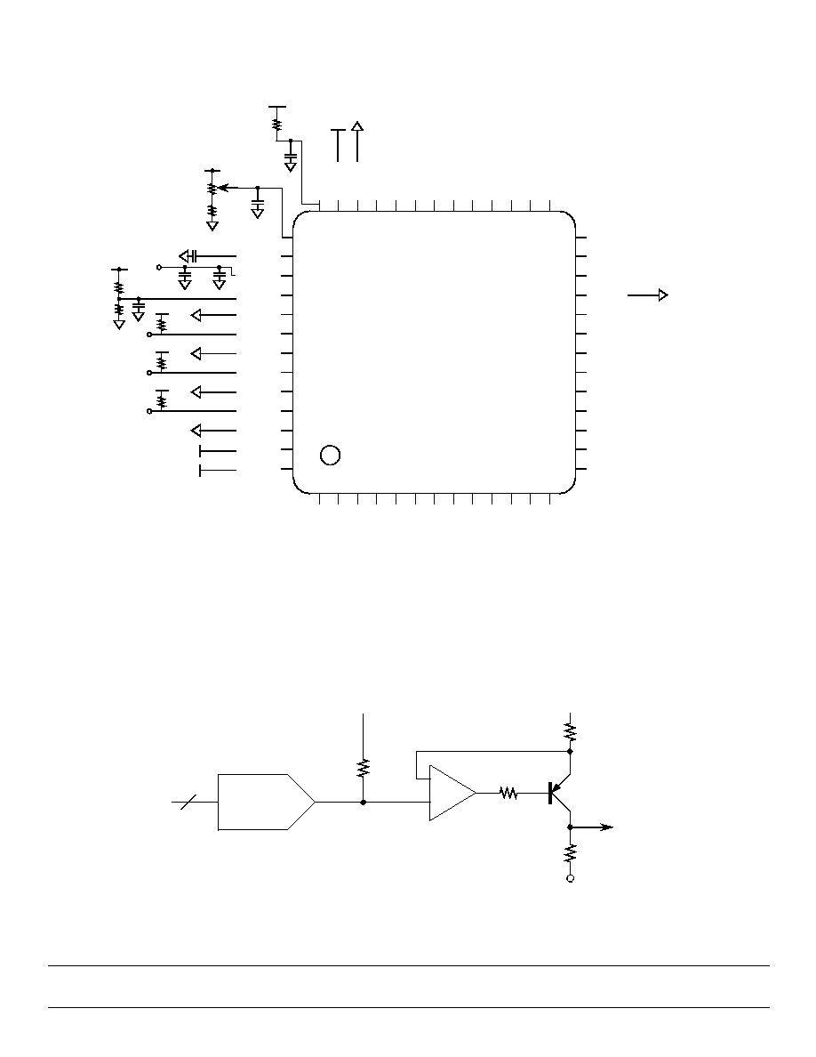
INTERFACE CONSIDERATIONS
Figure 4 shows a typical interface circuit of the SPT5230 in
normal circuit operation.
SUPPLY AND GROUND CONSIDERATIONS
Fairchild suggests that all power supply pins (AV
DD
) be tied
together and decoupled using a 0.1
µ
F ceramic capacitor in
parallel with a 10
µ
F tantalum capacitor.
EXTERNAL REFERENCE VOLTAGE (V
REF1
)
A +3 V (
±
10%) voltage reference should be externally gener-
ated for the V
REF1
pin using the simple voltage divider shown
in figure 4. Connect a 0.1
µ
F bypass capacitor between
V
REF1
and AV
SS
as close to the pin as possible.
EXTERNAL REFERENCE VOLTAGE (V
REF2
)
V
REF2
needs to be externally connected to AV
DD
through a
1.2 k
(5%) resistor. Connect a 0.1
µ
F bypass capacitor
between V
REF2
and AV
SS
as close to the pin as possible.
CONTROL VOLTAGE DECOUPLING (V
CS1
)
This is a decoupling pin for the control voltage internal
circuitry. An external 0.1
µ
F capacitor should be connected
between V
CS1
and AV
SS
as close to the pin as possible.
FULL-SCALE ADJUST CONTROL (V
CS2
)
V
CS2
is an external control voltage input that controls the
peak-to-peak full scale output voltage. This is the only exter-
nal voltage that has direct control over the SPT5230 output
voltage. The voltage output swings between AV
DD
(+5 V) and
a value controlled by V
CS2
.
Assuming that an output load resistor of 75
is connected
between the output and AV
DD
, figure 2 shows what the output
voltage will be for the digital inputs all equal to logic 0, as V
CS2
is varied from 2 V to 4 V. Figure 3 shows the peak-to-peak
output voltage versus V
CS2
and table I shows an example in
which V
CS2
is equal to 2.1 V.
CURRENT OUTPUTS
Each red, green and blue current output should have a load
resistor connected to AV
DD
. The resistors are typically 75
and should be kept in the 72
to 85
range. The outputs
should drive a high impedance load such as a voltage
follower.
OUTPUT LEVEL SHIFTING CIRCUIT
The SPT5230 voltage output will swing from +3.0 V to +4.99
V for V
CS2
= 2.1 V as shown in table I. If level shifting of the
output is desired, Fairchild recommends use of the circuit
shown in figure 5. The desired ≠FS voltage is fed into the
collector of the emitter to achieve the desired level shift. (Note
the phase inversion that will occur due to the common
emitter.) Choose any appropriate video op amp with ad-
equate power supply head room.
Table I ≠ Binary Codes
1 LSB = 1.953 mV, V
CS2
2.1 V
Digital Input
Analog
Step
A9 A8 A7 A6 A5 A4 A3 A2 A1 A0
Out (V)
(MSB)
(LSB)
0
0
0
0
0
0
0
0
0
0
0 3.000000
1
0
0
0
0
0
0
0
0
0
1 3.001953
2
0
0
0
0
0
0
0
0
1
0 3.003906
3
0
0
0
0
0
0
0
0
1
1 3.005859
.
.
.
.
.
.
.
.
.
1022
1
1
1
1
1
1
1
1
1
0 4.996094
1023
1
1
1
1
1
1
1
1
1
1 4.998047
4
5 / 1 / 0 0
SPT5230
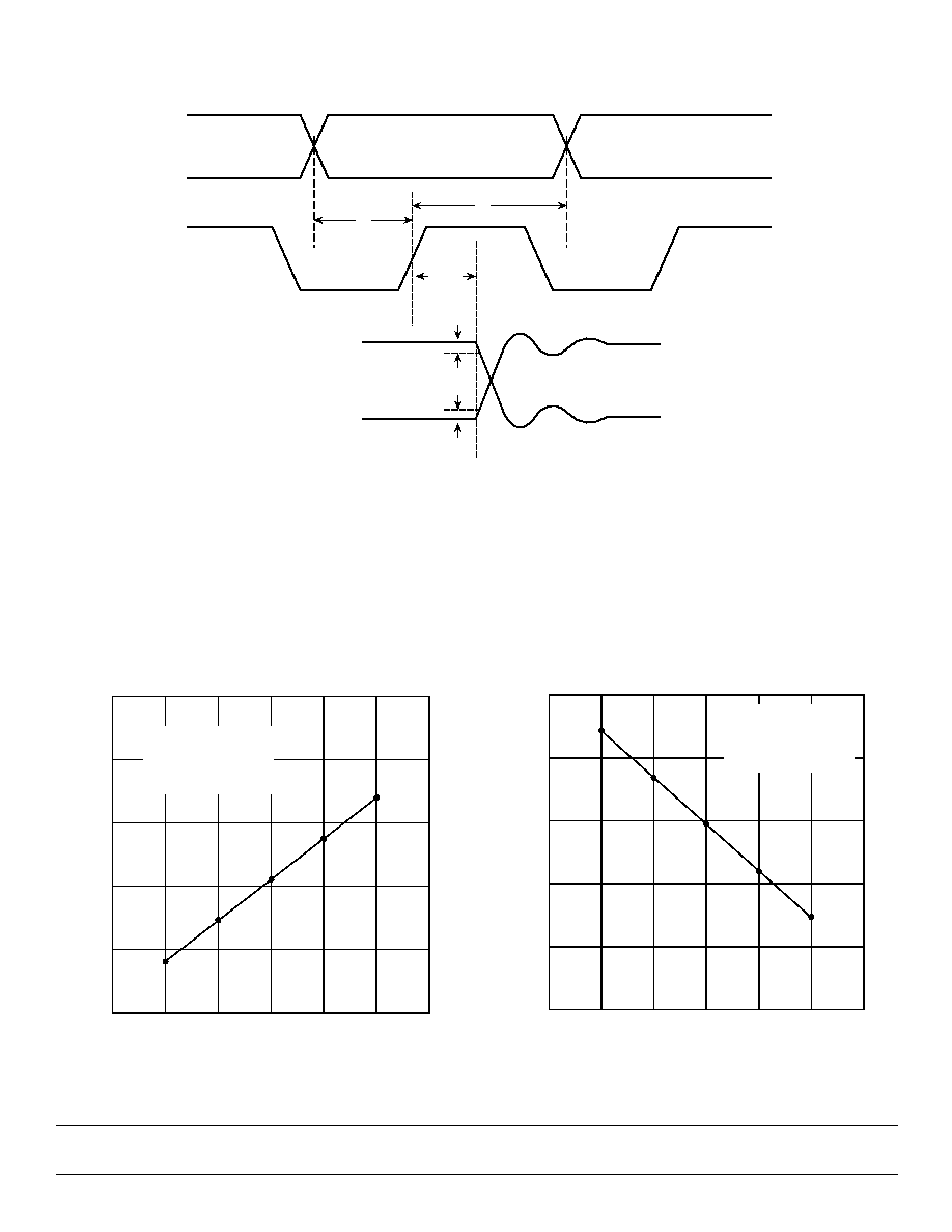
Figure 2 ≠ Output Voltage with All
Digital Inputs = ÿ versus V
CS2
Output V
oltage (V) (-FS)
V
CS2
(V)
4.0
3.5
3.0
2.5
2.0
1.5
2.5
3.0
3.5
4.0
4.5
5.0
Output Resistor = 75
T
A
= +25 ∞C
Digital Inputs = All ÿ
V
REF1
= 3 V
4.5
NOTE: For Digital Inputs = All 1, Output Voltage = +4.998047 V.
Figure 3 ≠ Output Voltage (Vp-p) versus V
CS2
Output V
oltage (Vp-p)
V
CS2
(V)
4.0
3.5
3.0
2.5
2.0
1.5
0.0
0.5
1.0
1.5
2.0
2.5
Output Resistor = 75
T
A
= +25 ∞C
V
REF1
= 3 V
4.5
Figure 1 ≠ Timing Diagram
th
N-Data
1/2 LSB
tpd
ts
N-Output Level
1/2 LSB
5
5 / 1 / 0 0
SPT5230
Figure 4 ≠ Typical Interface Circuit
SPT5230
26
25
24
23
22
21
20
19
18
17
16
15
14
40
41
42
43
44
45
46
47
48
49
50
51
52
27
28
29
30
31
32
33
34
35
36
37
38
39
13
12
11
10
9
8
7
6
5
4
3
2
1
G8
G9 (MSB)
N/C
Rÿ (LSB)
R1
R2
R3
R4
R5
R6
R7
R8
R9 (MSB)
B7
B8
B9 (MSB)
AVSS
N/C
Gÿ (LSB)
G1
G2
G3
G4
G5
G6
G7
B6
B5
B4
B3
B2
B1
Bÿ (LSB)
CLKB
CLKG
CLKR
AV
SS
AV
DD
V
REF2
VCS2
VCS1
AVDD
VREF1
AVSS
BOUT
AVSS
GOUT
AVSS
ROUT
AVSS
AVDD
AVDD
1.2 k
AVDD
0.1 µF
20 k
6 k
AVDD
0.1 µF
0.1 µF
0.1 µF
0.1 µ
F
10 µ
F
AVDD
75
AVDD
75
AVDD
75
+5 V
1.2 k
AVDD
0.75 k
Figure 5 ≠ Recommended Output Level Shifting Circuit
DAC
1 of 3
AV
D
D
75
-
+
Out
-FS
75
75
10
AV
D
D
10
NOTE: All three DACs use the
same circuit configuration.