
-
+
-
+
-
+
-
+
VOUT0
VOUT1
VOUT2
VOUT3
VOUT4
VOUT5
VOUT6
VOUT7
-
+
-
+
-
+
-
+
LE
D
Q
LEA7
LE
D
Q
7A
7B
LE
D
Q
LEA6
LE
D
Q
6A
6B
LE
D
Q
LEA5
LE
D
Q
5A
5B
LE
D
Q
LEA4
LE
D
Q
4A
4B
LE
D
Q
LEA3
LE
D
Q
3A
3B
LE
D
Q
LEA2
LE
D
Q
2A
2B
LE
D
Q
LEA1
LE
D
Q
1A
1B
LE
D
Q
LEA0
LE
D
Q
0A
0B
Control
Logic
WR
CS
A0A2
LDAC
LEA0LEA7
8
13
13
13
13
13
13
13
13
13
13
13
13
13
13
13
13
13
DAC0
DAC1
DAC2
DAC3
DAC4
DAC5
DAC6
DAC7
V
REFT01
V
REFB01
CLR
RGND
01
RGND
23
RGND
67
RGND
45
D0D12
LDAC
V
REFT2345
V
REFB2345
V
REFT67
V
REFB67
LDAC
LDAC
LDAC
LDAC
LDAC
LDAC
LDAC
LDAC
SPT5420
13-BIT, OCTAL D/A CONVERTER
TECHNICAL DATA
JUNE 26, 2001
FEATURES
∑ 13-bit resolution
∑ Pin compatible with AD7839
∑ Eight DACs in one package
∑ Buffered voltage outputs
∑ Wide output voltage swing V
DD
≠2.5 V to V
SS
+2.5 V
∑ 15 µs settling time to ±0.5 LSB
∑ Double-buffered digital inputs
∑ Microprocessor and TTL/CMOS compatible
APPLICATIONS
∑ Automatic test equipment
∑ Instrumentation
∑ Process control
GENERAL DESCRIPTION
The SPT5420 contains eight 13-bit digital-to-analog
CMOS converters designed primarily for automatic test
equipment applications. It uses novel circuit topology to
convert the 13-bit digital inputs into output voltages which
are proportionate to the applied reference voltages. Each
DAC's full-scale output voltage and output voltage offset
are adjustable with analog inputs (RGND, V
REFB
, V
REFT
).
The SPT5420 operates over an industrial temperature
range of ≠40 ∞C to +85 ∞C and is available in a 10 x 10 mm,
44-lead metric quad flat pack (MQFP) plastic package.
BLOCK DIAGRAM

2
6/26/01
SPT5420
ABSOLUTE MAXIMUM RATINGS (Beyond which damage may occur)
1
25 ∞C
Note: 1. Operation at any Absolute Maximum Rating is not implied. See
Electrical Specifications for proper nominal applied conditions
in typical applications.
ELECTRICAL SPECIFICATIONS
T
A
= T
MIN
to T
MAX
, V
CC
= +5.0 V, V
DD
= +11.5 V, V
SS
= ≠8.0 V, V
REFT
=3.5 V, V
REFB
= ≠1.5 V, R
L
= +10 k
, C
L
= 50 pF, unless otherwise specified.
TEST
TEST
SPT5420
PARAMETERS
CONDITIONS
LEVEL
MIN
TYP
MAX
UNITS
Accuracy
Resolution
VI
13
Bits
Integral Linearity Error (ILE)
VI
≠2.0
±0.5
+2.0
LSB
Differential Linearity Error (DLE)
VI
≠1.0
±0.3
+1.0
LSB
Zero-Scale Error
VI
≠25
+25
mV
Full Scale Error
VI
≠25
+25
mV
Gain Error
VI
≠25
+25
mV
Reference Inputs
Input Current
IV
±100
nA
V
REFT1
VI
0
+3.5
+5.0
V
V
REFB2
VI
≠5.0
≠1.5
0
V
RGND Inputs
DC Input Impedance
V
60
k
Input Range
IV
≠2.0
2.0
V
Output Characteristics
Output Swing
3,4
VI
+7/≠3
V
Short Circuit Current
IV
15
mA
Resistive Load
VI
5
k
DC Output Impedance
IV
1.0
Digital Inputs
Logic 1 Voltage
VI
2.4
V
Logic 0 Voltage
VI
0.8
V
Maximum Input Current
VI
≠10
10
µA/pin
Input Capacitance
V
10
pF
Supply Voltages
V
CC
........................................................................ +6 V
V
DD
...................................................................... +15 V
V
SS
...................................................................... ≠15 V
Input Voltages
V
REFT
.................................... V
SS
≠0.3 V to V
DD
+0.3 V
V
REFB
................................... V
DD
+0.3 V to V
SS
≠0.3 V
Digital inputs .................................... ≠0.3 V to V
CC
+0.3 V
Temperature
Operating Temperature .......................... ≠40 to +85 ∞C
Storage ................................................ ≠65 to +150 ∞C
Notes:
1. V
REFT
< 8 V + (V
SS
x 0.5); e.g., if V
SS
= ≠8 V, then V
REFT
< 4 V
2. V
REFB
> (V
DD
x 0.5) ≠ 9.5 V; e.g., if V
DD
= 11 V, then V
REFB
> ≠4 V
3. V
SS
+ 2.5 V
V
OUT
V
SS
+ 16.0 V for 18.5 V
V
DD
≠ V
SS
20.0 V
V
SS
+ 2.5 V
V
OUT
V
DD
≠ 2.5 V for V
DD
≠ V
SS
18.5 V
4. V
OUT
= 2 X (V
REFB
+[V
REFT
≠ V
REFB
] X
INPUT CODE
8192
) ≠ V
RGND

3
6/26/01
SPT5420
TEST LEVEL CODES
All electrical characteristics are subject to the
following conditions:
All parameters having min/max specifications
are guaranteed. The Test Level column indi-
cates the specific device testing actually per-
formed during production and Quality Assur-
ance inspection. Any blank section in the data
column indicates that the specification is not
tested at the specified condition.
LEVEL
TEST PROCEDURE
I
100% production tested at the specified temperature.
II
100% production tested at T
A
= +25 ∞C, and sample tested at the
specified temperatures.
III
QA sample tested only at the specified temperatures.
IV
Parameter is guaranteed (but not tested) by design and characteri-
zation data.
V
Parameter is a typical value for information purposes only.
VI
100% production tested at T
A
= +25 ∞C. Parameter is guaranteed
over specified temperature range.
ELECTRICAL SPECIFICATIONS
T
A
= T
MIN
to T
MAX
, V
CC
= +5.0 V, V
DD
= +11.5 V, V
SS
= ≠8.0 V, V
REFT
=3.5 V, V
REFB
=≠1.5 V, R
L
= +10 k
, C
L
= 50 pF, unless otherwise specified.
TEST
TEST
SPT5420
PARAMETERS
CONDITIONS
LEVEL
MIN
TYP
MAX
UNITS
Power Requirements
V
CC
Supply Voltage (Digital)
IV
4.75
5
5.25
V
V
DD
Supply Voltage (Analog)
1,2
VI
5
11.5
12.5
V
V
SS
Supply Voltage (Analog)
1,2
VI
≠12.5
≠8
≠5
V
I
CC
Supply Current
VI
0.5
mA
I
DD
Supply Current
Outputs Unloaded
VI
5
10
mA
I
SS
Supply Current
Outputs Unloaded
VI
5
10
mA
Power Supply Rejection Ratio
V
DD
/
Full Scale
IV
80
dB
V
SS
/
Full Scale
IV
80
dB
Dynamic Performance
Output Settling Time
3
(Full Scale Change to ±0.5 LSB) C
L
220 pF
IV
15
µs
Slew Rate
V
2.0
V/µs
Glitch Impulse
V
35
nV-s
Channel to Channel Isolation
V
100
dB
DAC to DAC Crosstalk
V
40
nV-s
Digital Crosstalk
V
1
nV-s
Digital Feedthrough
V
1
nV-s
Timing Characteristics
(See page 4)
IV
1. Supplies should provide 2.5 V headroom above and below max output swing.
2. V
DD
≠ V
SS
20 V
3. Output can drive 10,000 pF without oscillation, but with settling time degradation.
DEFINITION OF SELECTED TERMINOLOGY
Channel-to-Channel Isolation
Channel-to-Channel isolation refers to the proportion of input signal from one DAC's reference input that appears at the output of
the other DAC. It is expressed in dBs.
DAC-to-DAC Crosstalk
DAC-to-DAC crosstalk is defined as the glitch impulse that appears at one DAC's output due to both the digital change and subse-
quent analog output change at any other DAC. It is specified in nV-s.
Digital Crosstalk
The glitch impulse transferred to one DAC's output due to a change in digital input code of any other DAC. It is specified in nV-s.
Digital Feedthrough
Digital feedthrough is the noise at a DAC's output caused by changes to D0≠D12 while
WR
is high.
4
6/26/01
SPT5420
PARAMETER
SYMBOL
MIN
TYP
MAX
UNIT
Address Valid to
WR
Setup
t
1
20
ns
Address Valid to
WR
Hold
t
2
0
ns
CS
Pulse Width Low
t
3
50
ns
WR
Pulse Width Low
t
4
50
ns
CS
to
WR
Setup
t
5
0
ns
WR
to
CS
Hold
t
6
0
ns
Data Setup
t
7
25
ns
Data Hold
t
8
0
ns
Settling Time
1
t
9
15
us
LDAC
Pulse Width Low
t
10
50
ns
CLR
Pulse Activation
t
11
300
ns
NOTES:
All digital input rise and fall times are measured from 10% to 90% of +5 V.
t
r
= t
f
= 5 ns.
1. R
L
= 10 k
C
L
220 pF
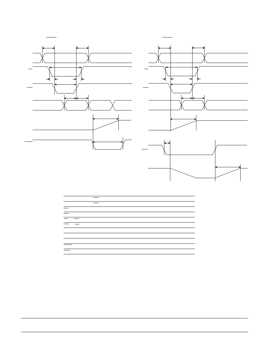
TIMING CHARACTERISTICS
t
5
t
3
t
6
t
4
t
1
t
2
t
7
t
8
t
10
CS
WR
A0A2
D0D12
LDAC
t
9
V
OUT
t
5
t
3
t
6
t
4
t
1
t
2
t
7
t
8
CS
WR
A0A2
D0D12
t
9
V
OUT
t
11
t
9
CLR
V
OUT
Figure 1a ≠ Timing Diagram: Latched Mode
(
LDAC
Strobed)
Figure 1b ≠ Timing Diagram: Transparent Mode
(
LDAC
Held Low)

5
6/26/01
SPT5420
VOLTAGE REFERENCES AND
ANALOG GROUND INPUTS
Three V
REFTXX
and three V
REFBXX
inputs set the output
range of the three corresponding groups of DACs
(0 and 1; 2 through 5; 6 and 7). Four RGND
XX
inputs set
the output offset voltage of the four corresponding groups
of DACs (0 and 1; 2 and 3; 4 and 5; 6 and 7). The formula
for output swing and offset is presented in the "Analog
Outputs" section below.
DAC ADDRESSING AND LATCHING
Each DAC has an input latch which receives data from the
data bus, and a DAC latch which receives data from the
input latch. The analog output of each DAC corresponds
to the data in its DAC latch. One of the eight input latches
is addressed by the address lines A(2:0) according to
Table I. While
CS
and
WR
are low, the addressed input
latch is transparent and the seven other input latches are
latched. Bringing
CS
or
WR
high latches data into the ad-
dressed input latch. While
LDAC
is low, all eight DAC
latches are transparent. Bringing
LDAC
high latches data
into the DAC latches. While
CS
,
WR
and
LDAC
are low, both
latches are transparent and input data is transferred
directly to the selected DAC. While
CLR
is low, all DAC out-
puts are set to their corresponding RGND
XX
. Bringing
CLR
high returns each DAC's output to the voltage correspond-
ing to the data in each DAC latch.
Table II summarizes this information, and figures 1a and
1b should be referenced for timing limitations.
POWER SUPPLY SEQUENCING
The sequence in which V
DD
, V
SS
and V
CC
come up is not
critical. The reference inputs, V
REFTXX
and V
REFBXX
, must
come on only after V
DD
and V
SS
have been established.
However, they may be turned on prior to V
CC
. The digital
inputs must be driven only after V
DD
, V
SS
and V
CC
have
been established. Reverse the power-on sequence for
power-down.
ANALOG OUTPUTS VS DIGITAL INPUT
CODE
The output voltage range is equal to twice the difference
between V
REFTXX
and V
REFBXX
. The output voltage is
given by:
V
OUT
= 2 X (V
REFB
+[V
REFT
≠ V
REFB
] X
INPUT CODE
8192
) ≠ V
RGND
CODE = 0 ≠ 8191
Table I ≠ DAC Addressing
Addressed Input
A2
A1
A0
Latch DAC#
0
0
0
0
0
0
1
1
0
1
0
2
0
1
1
3
1
0
0
4
1
0
1
5
1
1
0
6
1
1
1
7
Table II ≠ Control Logic Table
WR
CS
LDAC
CLR
Input Latch DAC Latch
0
0
x
1
transparent
1
x
1
x
x
1
latched
x
x
1
x
1
latched
x
x
x
0
1
x
transparent
x
x
1
1
x
latched
x
x
x
0
DAC outputs at RGND
XX
Note:
1. Only the input latch addressed by A(2:0) is transparent.
The other input latches are latched.