 | –≠–ª–µ–∫—Ç—Ä–æ–Ω–Ω—ã–π –∫–æ–º–ø–æ–Ω–µ–Ω—Ç: SPT5510 | –°–∫–∞—á–∞—Ç—å:  PDF PDF  ZIP ZIP |
SPT5510
16-BIT, 200 MWPS ECL D/A CONVERTER
APPLICATIONS
∑ High-precision arbitrary waveform generation
∑ Test and measurement instrumentation
∑ Digital waveform synthesis
∑ Microwave and satellite modems
∑ Disk drive test equipment
∑ Industrial process control
∑ Military applications
BLOCK DIAGRAM
GENERAL DESCRIPTION
The SPT5510 is a 16-bit, 200 MWPS digital-to-analog
converter designed for high-resolution waveform synthesis
for test and measurement instrumentation applications. It
features true 16-bit linearity, with differential non-linearity of
typically
±
0.6 LSB and integral non-linearity of
±
0.75 LSB. It
FEATURES
∑ 16-Bit, 200 MWPS digital-to-analog converter
∑ Differential linearity of
±
0.6 LSB (typical)
∑ Integral linearity of
±
0.75 LSB (typical)
∑ Fast settling time: 35 ns to 0.0008%; 25 ns to 0.01%
∑ Low glitch energy
∑ On-chip voltage reference
∑ ECL compatibility
has a very high-speed update rate of up to 200 MHz and is
ECL compatible. It has an ultrafast settling time of 25 ns to
0.01% and 35 ns to 0.0008%.
The SPT5510 operates over an industrial temperature
range of ≠40
∞
C to +85
∞
C and is available in a 10 x 10 mm,
44-lead metric quad flat pack (MQFP) plastic package.
16
16
12
12
16
I
OUT
I
OUT
CLK
Digital Inputs
D15≠D0
Bandgap
Reference
BG
OUT
R
SET
AMP
INB
+
≠
Ref
Amp
AMP
OUT
AMP
CC
20
10
Bias
Reference
Cell
Bias
Current
Cells
D15≠D12
D11≠D0
MSB Latch
LSB Latch
Input
Latch
MSB
Decoder
LSB
Buffer
I
OUT
I
OUT
REF
IN

2
9 / 2 7 / 0 0
SPT5510
DC Performance
1
Resolution
16
Bits
Differential Linearity
VI
≠1.95
±
0.6
1.95
LSB
Differential Linearity
T
MIN
≠T
MAX
IV
≠4.0
±
1.0
4.0
LSB
Integral Linearity
VI
≠1.95
±
0.75
1.95
LSB
Integral Linearity
T
MIN
≠T
MAX
IV
≠4.0
±
1.5
4.0
LSB
Integral Linearity Drift
IV
≠0.2
0.2
LSB/
∞
C
Offset Drift
T
MIN
≠T
MAX
IV
≠2.5
2.5
ppm FS/
∞
C
Monotonicity
V
15
Bits
Output Capacitance
V
10
pF
Gain Error
I
≠2
0.4
2
% FS
Gain Error Tempco
With Ext Reference
V
50
ppm FS/
∞
C
Gain Error Tempco
With Internal Bandgap Ref
V
50
ppm FS/
∞
C
Offset Error
I
≠4
4
µ
A
Compliance Voltage
IV
≠1.2
2
V
Output Resistance
IV
0.88
1.1
1.32
k
Dynamic Performance
Conversion Rate
IV
200
MHz
Settling Time t
ST2
Settling to
±
0.01%
V
25
ns
Settling to
±
0.0008%
V
35
ns
Delay Time t
D
V
2
ns
Glitch Energy
V
30
pV-s
Full Scale Output Current
With On-Chip References
V
19
mA
Rise Time/Fall Time
R
L
= 50
V
2
ns
Spurious Free Dynamic Range
OUT
=5 MHz;
CLOCK
=30 MHz
10 MHz Span
V
84
dB
OUT
=10 MHz;
CLOCK
=100 MHz
10 MHz Span
V
76
dB
ABSOLUTE MAXIMUM RATINGS (Beyond which damage may occur)
1
Supply Voltages
Negative supply voltage (V
EE
) ................................. ≠7 V
A/D ground voltage differential ................................ 0.5 V
Input Voltages
Digital input voltage (D15≠D0, Clock)... ........... ≠2.5 to 0 V
Ref amp input voltage range .......................... ≠2.5 to 0 V
Reference input voltage range (Ref In) ...... V
EE
to ≠2.5 V
Output Currents
Bandgap reference output current .....................
±
500
µ
A
Ref amplifier output current ................................
±
2.5 mA
Temperature
Operating temperature ............................... ≠40 to +85
∞
C
Junction temperature .......................................... +150
∞
C
Lead, soldering (10 seconds) ............................. +250
∞
C
Storage .................................................... ≠65 to +150
∞
C
ELECTRICAL SPECIFICATIONS
T
A
= 25
∞
C, V
EE
=≠5.2 V
±
5%, 50% duty cycle clock, unless otherwise specified.
TEST
TEST
SPT5510
PARAMETERS
CONDITIONS
LEVEL
MIN
TYP
MAX
UNITS
Note: 1. Operation at any Absolute Maximum Rating is not implied. See Electrical Specifications for nominal operating
conditions.
1
Measured at 0 V output using I-V.
2
Measured as voltage settling for mid-scale transition; R
L
= 50
.

3
9 / 2 7 / 0 0
SPT5510
ELECTRICAL SPECIFICATIONS
T
A
= 25
∞
C, V
EE
=≠5.2 V
±
5%, 50% duty cycle clock, unless otherwise specified.
TEST
TEST
SPT5510
PARAMETERS
CONDITIONS
LEVEL
MIN
TYP
MAX
UNITS
Power Supply Requirements
Negative Supply Current (≠5.2 V)
T
MIN
≠T
MAX
VI
115
150
mA
Nominal Power Dissipation
V
600
800
mW
Power Supply Rejection Ratio
V Supply =
±
5 %
I
≠0.6
±
0.002
0.6
% FS
Voltage Input and Control
Bandgap Reference Voltage
V
≠1.2
V
Bandgap Output Current
T
A
=25
∞
C
±
10
∞
C
IV
≠110
16
220
µ
A
Ref Amp Bandwidth
3
V
40
MHz
Ref Amp Input Current
V
16
µ
A
Ref Amp Output Current
V
200
µ
A
Ref In Operating Voltage
V
≠3.4
V
Digital Inputs
Logic 1 Voltage
T
MIN
≠T
MAX
VI
≠1.0
≠0.8
V
Logic 0 Voltage
T
MIN
≠T
MAX
VI
≠1.7
≠1.5
V
Logic 1 Current
≠0.8 V
V
2.5
µ
A
Logic 0 Current
≠1.8 V
V
0
µ
A
Input Capacitance
V
3
pF
Input Setup Time (t
S
)
IV
3.0
ns
Input Hold Time (t
H
)
IV
0.5
ns
Clock Pulse Width (t
PWH
)
IV
1.5
ns
3
Ref Amp Bandwidth is limited by its compensation network
TEST LEVEL CODES
All electrical characteristics are subject
to the following conditions:
All parameters having min/max specifi-
cations are guaranteed. The Test Level
column indicates the specific device
testing actually performed during pro-
duction and Quality Assurance inspec-
tion. Any blank section in the data
column indicates that the specification
is not tested at the specified condition.
TEST LEVEL
TEST PROCEDURE
I
100% production tested at the specified temperature.
II
100% production tested at T
A
= +25
∞
C, and sample tested at the specified
temperatures.
III
QA sample tested only at the specified temperatures.
IV
Parameter is guaranteed (but not tested) by design and characterization
data.
V
Parameter is a typical value for information purposes only.
VI
100% production tested at T
A
= +25
∞
C. Parameter is guaranteed over
specified temperature range.

4
9 / 2 7 / 0 0
SPT5510
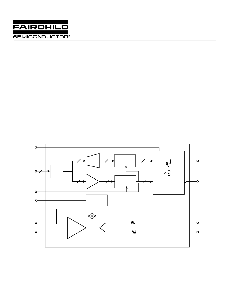
THEORY OF OPERATION
The SPT5510 is a segmented 16-bit current-output DAC.
The four MSBs, D15≠D12, are decoded to fifteen unit cells
(current sinks). The remaining bits (D11≠D0) are binary;
bits D9≠D0 are derived from an R-2R ladder. All cells are
laser trimmed for maximum accuracy. The block diagram
shows the basic architecture.
All output cells are always on, with the data determining
whether a given cell's current is routed from I
OUT
or I
OUT
.
This provides nearly constant power dissipation indepen-
dent of data and clock rate. It also reduces noise transients
on power and ground lines.
The reference loop utilizes an MSB-weighted cell and pro-
vides a gain of about 16 to the output. The on-chip refer-
ence amplifier has very high open-loop gain and is offset
trimmed to provide a very low temperature drift (typically
<10 ppm/
∞
C gain drift).
POWER SUPPLY AND GROUNDING
The SPT5510 requires a single ≠5.2V power supply. All
supply pins attach to a common on-chip power bus and
should be treated as analog supplies. For best settling per-
formance, each supply pin should be decoupled as shown
in figure 1 ≠ typical interface circuit.
There are three separate on-chip ground busses. DGND
pins should be tied together and connected to system
ground through a ferrite bead. REFGND and OGND pins
should be tied directly to the SPT5510's ground plane and
connected to system ground through a ferrite bead. It is
critical that REFGND and OGND are very tightly coupled,
as any differential signal (dc offset, noise, etc.) will be
transmitted to the output. Two of the OGND pins can be
disconnected from the ground plane and used as sense
lines for a current-to-voltage converter, as shown in the
OUTPUTS section.
DGND
DGND
DGND
DGND
OGND
OGND
OGND
OGND
AV
EE
AV
EE
AV
EE
AV
EE
AV
EE
AV
EE
AV
EE
AV
EE
C1
C2
C3
C4
C5
.01
µ
F
.01
µ
F
.01
µ
F
.01
µ
F
.01
µ
F
R1
R2
R3
R4
R5
R6
10
10
10
10
10
10
C17
C16
C15
C14
2.2
µ
F
2.2
µ
F
2.2
µ
F
2.2
µ
F
10
44
24
33
40
42
35
37
39
43
11
13
14
23
34
38
1
2
3
4
5
6
7
8
25
26
27
28
29
30
31
32
D15
D14
D13
D12
D11
D10
D9
D8
D7
D6
D5
D4
D3
D2
D1
D0
C6
.01
µ
F
C11
47 pF
C10
47 pF
C9
47 pF
C8
.01
µ
F
C7
.01
µ
F
C12
10 pF
C13
20 pF
50
R9
50
R8
1K
R7
1K
REFGND
REFGND
CLK
BG
OUT
AMP
INB
R
SET
AMP
CC
AMP
B
AMP
OUT
REF
IN
I
OUT
I
OUT
9
22
12
16
18
17
19
15
20
21
41
36
C1≠C13 -- SURFACE MOUNT CERAMIC CHIP
C14≠C17 -- TANTALUM
R1≠R6 -- CARBON FILM 1/4 W
R7≠R10 -- SURFACE MOUNT CERAMIC CHIP
FB -- FERRITE BEAD is to be located as closely
to the device as possible.
SPT5510
AV
EE
R10
FB
AV
EE
Input
Data
Output
Complementary
Output
Figure 1 ≠ Typical Interface Circuit
5
9 / 2 7 / 0 0
SPT5510
Wideband decoupling is required for optimum settling per-
formance. This may require several capacitors in parallel,
and series resistors when appropriate, to reduce resonance
effects. Some applications may need only a single capaci-
tor; however, decoupling influences both long- and short-
term settling, so caution is urged. Your application may
require some research to determine the optimum power
supply decoupling network.
DIGITAL INPUTS AND TIMING
Each digital input is buffered, decoded, and then latched
into D flip-flops which drive the output switches. Master-
slave flip-flops are not used; thus, there is only a 1/2 clock
period delay (max) from data change to output change. In
this architecture, clock and data edge speeds (i.e., rise/fall
times) may affect data feedthrough. Using a data edge of
approximately 0.8 ns will cause data feedthrough of about
10 pV-s, while a 5 ns data edge will reduce the feedthrough
to about 4 pV-s. Data lines may include series resistors or
RC filters for edge control if desired.
The clock signal controls when the data is latched into the
flip-flops. When the CLK is high, the DAC is in track mode. A
negative going CLK latches the data. If CLK is held low, the
DAC is in hold mode. See figure 2.
OUTPUTS
The output is comprised of current sinks, R-2R ladder, and
associated parasitics. See figure 3 for an equivalent output
circuit.
The DAC's full-scale output current when using the internal
reference amplifier is determined by the voltage at pin
AMP
INB
and the R
SET
resistance. It can be found (to within
an LSB) by using the following formula:
I
OUT
FS = (AMP
INB
/R
SET
) x 16
The inputs determine whether the current from each sink
comes from I
OUT
or I
OUT
as follows:
Code (D15 is MSB)
I
OUT
I
OUT
0 (zero scale)
No current
All current
32768 (mid-scale)
I
OUT
= I
OUT
I
OUT
= I
OUT
65535 (full-scale)
All current
No current
Differential outputs facilitate maximum noise rejection and
signal swing. The DAC is trimmed using a current to voltage
(I-V) converter which provides a virtual ground at the out-
puts and includes sense lines to mitigate the impact of bus
drops. Operating into a load other than a virtual ground will
introduce a slight bow at the output. This bow is related to
the current sinks' finite output impedance and ladder
impedance.
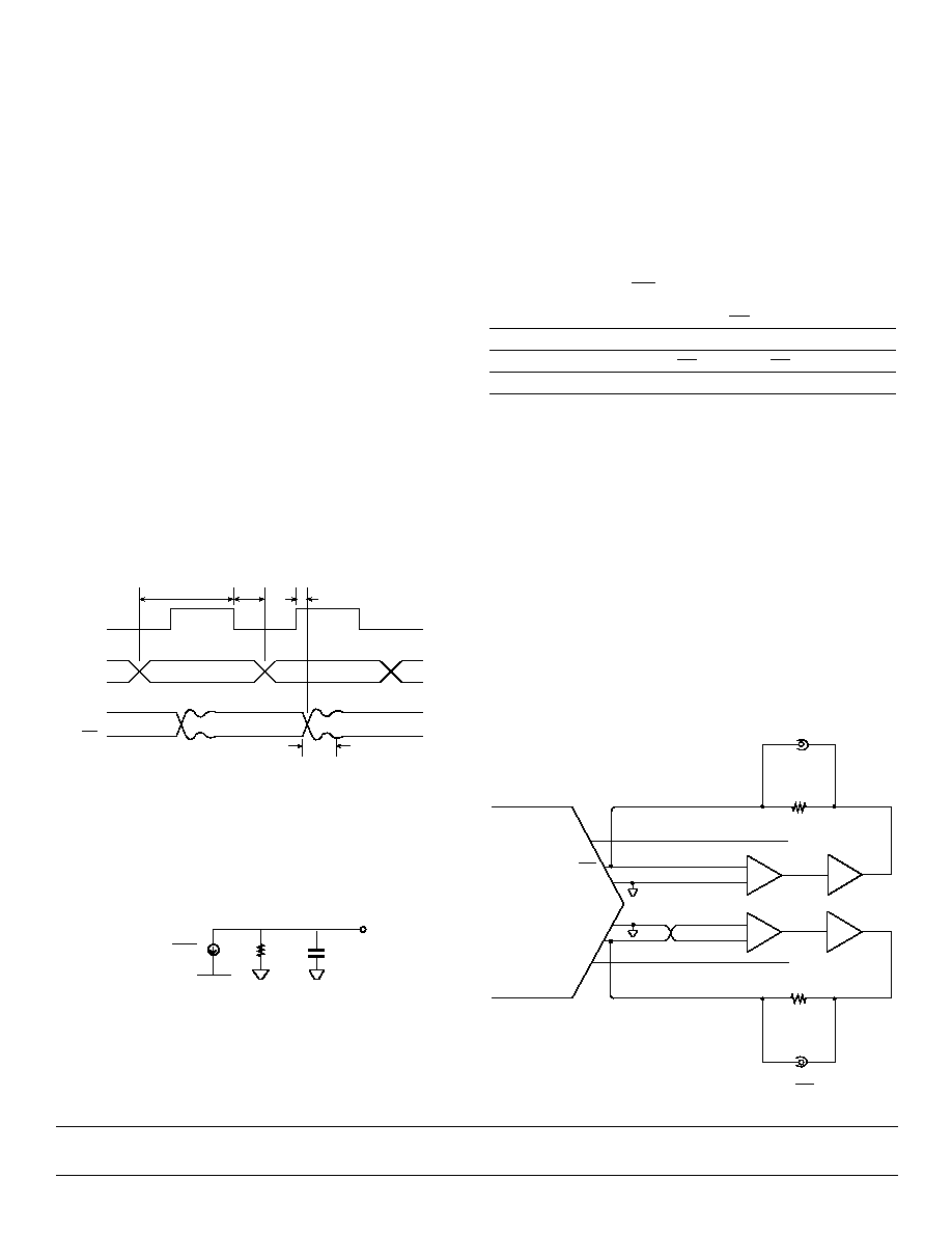
An example circuit using an I-V converter is shown in figure
4. Note that resistor and op-amp self heating over the DAC's
full-scale range will introduce additional temperature depen-
dence. The op-amp and feedback resistor must both have
very low tempcos if the DAC's intrinsic gain drift is to be
maintained. A sense line helps reduce wire effects ≠ both IR
loss and temperature drift.
Figure 2 ≠ Timing Diagram
CLK
DATA
I
OUT
t
D
t
H
t
ST
I
OUT
t
S
t
H
= hold time
t
D
= time to output valid
t
S
= setup time
t
ST
= settling time
Figure 3 ≠ Equivalent Output Circuit
10 pF
1.1k
AV
EE
I
OUT
or I
OUT
+
≠
+
≠
OGND
OGND
OGND
OGND
GND
GND
250
250
BNC
"I
OUT
"
I
OUT
BNC
"I
OUT
"
I
OUT
Figure 4 ≠ I-V Converter