
SPT7710
8-BIT, 150 MSPS, FLASH A/D CONVERTER
TECHNICAL DATA
AUGUST 17, 2001
FEATURES
∑ Metastable errors reduced to 1 LSB
∑ Low input capacitance: 10 pF
∑ Wide input bandwidth: 210 MHz
∑ 150 MSPS conversion rate
∑ Typical power dissipation: 2.2 watts
APPLICATIONS
∑ Digital oscilloscopes
∑ Transient capture
∑ Radar, EW, ECM
∑ Direct RF down-conversion
∑ Medical electronics: ultrasound, CAT instrumentation
GENERAL DESCRIPTION
The SPT7710 is a monolithic flash A/D converter capable
of digitizing a two volt analog input signal into 8-bit digital
words at a 150 MSPS (typ) update rate.
For most applications, no external sample-and-hold is re-
quired for accurate conversion due to the device's narrow
aperture time, wide bandwidth, and low input capacitance.
A single standard ≠5.2 volt power supply is required for
operation of the SPT7710, with nominal power dissipation
of 2.2 W. A proprietary decoding scheme reduces meta-
stable errors to the 1 LSB level.
The SPT7710 is available in 42-lead ceramic sidebrazed
DIP, surface-mount 44-lead cerquad and 46-lead PGA
packages; the cerquad and PGA packages allow access
to additional reference ladder taps, an overrange bit, and a
data ready output. The SPT7710 is available in the indus-
trial temperature range.
256
255
152
151
128
127
64
63
2
1
256 to
8-Bit
Encoder
ECL
Latches
and
Buffers
AGND
Analog Input
(Sense or Force)
VEE
CLK
CLK
V
RBF
Convert
V
RBS
V
R1
V
R3
V
RTS
V
RTF
V
R2
2
Analog Input
(Force or Sense) AGND DGND
V
EE
LINV MINV
DRINV
DREAD
Overrange
D7 MSB
D6
D5
D4
D3
D2
D1
D0 LSB
MSB D7
D6
D5
D4
D3
D2
D1
LSB D0
These functions are
available in the PGA and
cerquad packages only.
Clock
Buffer
Preamp
Comparator
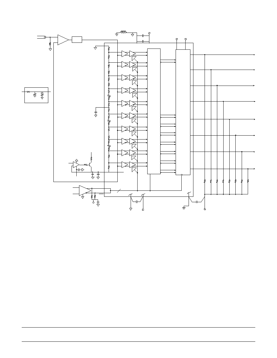
BLOCK DIAGRAM

2
8/17/01
SPT7710
ABSOLUTE MAXIMUM RATINGS (Beyond which damage may occur)
1
25 ∞C
Note: 1. Operation at any Absolute Maximum Rating is not implied. See
Electrical Specifications for proper nominal applied conditions
in typical applications.
Supply Voltages
Negative Supply Voltage (V
EE
TO GND) ≠7.0 to +0.5 V
Ground Voltage Differential .................... ≠0.5 to +0.5 V
Input Voltage
Analog Input Voltage ............................... V
EE
to +0.5 V
Reference Input Voltage .......................... V
EE
to +0.5 V
Digital Input Voltage ................................ V
EE
to +0.5 V
Reference Current V
RTF
to V
RBF
........................ 25 mA
Output
Digital Output Current ............................... 0 to ≠30 mA
Temperature
Operating Temperature,ambient ............. ≠25 to +85 ∞C
junction ...................... +150 ∞C
Lead Temperature, (soldering 10 seconds) ..... +300 ∞C
Storage Temperature ............................ ≠65 to +150 ∞C
ELECTRICAL SPECIFICATIONS
T
A
= T
MIN
to T
MAX
, V
EE
=≠5.2 V, R
Source
=50
, V
RBF
=≠2.00 V, V
R2
=≠1.00 V, V
RTF
=0.00 V,
CLK
=125 MHz, Duty Cycle=50%, unless otherwise specified.
TEST
TEST
SPT7710A
SPT7710B
PARAMETERS
CONDITIONS
LEVEL
MIN
TYP
MAX
MIN
TYP
MAX
UNITS
DC Accuracy
Integral Linearity Error
CLK
= 100 kHz
VI
≠0.75
±0.60
+0.75
≠0.95
±0.80
+0.95
LSB
Differential Linearity Error
CLK
= 100 kHz
VI
≠0.75
+0.75
≠0.95
+0.95
LSB
No missing codes
Guaranteed
Guaranteed
Analog Input
Offset Error V
RT
VI
≠30
+30
≠30
+30
mV
Offset Error V
RB
VI
≠30
+30
≠30
+30
mV
Input Voltage Range
VI
≠2.0
0.0
≠2.0
0.0
Volts
Input Capacitance
Over full
input range
V
10
10
pF
Input Resistance
V
15
15
k
Input Current
VI
250
500
250
500
µA
Input Slew Rate
V
1,000
1,000
V/µs
Large Signal Bandwidth
V
IN
=F.S.
V
210
210
MHz
Small Signal Bandwidth
V
IN
=500 mV
P-P
V
335
335
MHz
Clock Synchronous
Input Currents
V
40
40
µA
Reference Input
Ladder Resistance
VI
100
200
300
100
200
300
Reference Bandwidth
V
10
10
MHz
Timing Characteristics
Maximum Sample Rate
IV
125
150
125
150
MSPS
Clock to Data Delay
V
2.4
2.4
ns
Output Delay Tempco
V
2
2
ps/∞C
CLK-to-Data Ready Delay (t
D
)
V
2.0
2.0
ns
Aperture Jitter
V
5
5
ps
Acquisition Time
V
1.5
1.5
ns
Dynamic Performance
Signal-to-Noise Ratio
IN
= 3.58 MHz
VI
46
48
45
47
dB
IN
= 50 MHz
VI
42
46
40
44
dB
Total Harmonic Distortion
IN
= 3.58 MHz
VI
≠52
≠48
≠50
≠46
dB
IN
= 50 MHz
VI
≠44
≠40
≠43
≠39
dB
Signal-to-Noise and Distortion
IN
= 3.58 MHz
VI
45
48
43
46
dB
(SINAD)
IN
= 50 MHz
VI
39
42
37
40
dB

3
8/17/01
SPT7710
TEST LEVEL CODES
All electrical characteristics are subject to the
following conditions:
All parameters having min/max specifications
are guaranteed. The Test Level column indi-
cates the specific device testing actually per-
formed during production and Quality Assur-
ance inspection. Any blank section in the data
column indicates that the specification is not
tested at the specified condition.
Unless otherwise noted, all test are pulsed
tests; therefore, T
J
= T
C
= T
A
.
LEVEL
TEST PROCEDURE
I
100% production tested at the specified temperature.
II
100% production tested at T
A
= +25 ∞C, and sample tested at the
specified temperatures.
III
QA sample tested only at the specified temperatures.
IV
Parameter is guaranteed (but not tested) by design and characteri-
zation data.
V
Parameter is a typical value for information purposes only.
VI
100% production tested at T
A
= +25 ∞C. Parameter is guaranteed
over specified temperature range.
ELECTRICAL SPECIFICATIONS
T
A
= T
MIN
to T
MAX
, V
EE
=≠5.2 V, R
Source
=50
, V
RBF
=≠2.00 V, V
R2
=≠1.00 V, V
RTF
=0.00 V,
CLK
=125 MHz, Duty Cycle=50%, unless otherwise specified.
TEST
TEST
SPT7710A
SPT7710B
PARAMETERS
CONDITIONS
LEVEL
MIN
TYP
MAX
MIN
TYP
MAX
UNITS
Digital Inputs
Digital Input High Voltage
(MINV, LINV)
VI
≠1.1
≠0.7
≠1.1
≠0.7
Volts
Digital Input Low Voltage
(MINV, LINV)
VI
≠2.0
≠1.5
≠2.0
≠1.5
Volts
Clock Low Width, t
PWL
VI
4
5
4
5
ns
Clock High Width, t
PWH
VI
4
5
4
5
ns
Digital Outputs
Digital Output High Voltage
50
to ≠2 V
VI
≠1.1
≠1.1
Volts
Digital Output Low Voltage
50
to ≠2 V
VI
≠1.5
≠1.5
Volts
Power Supply Requirements
Supply Current
+25 ∞C
VI
425
550
425
550
mA
Power Dissipation
+25 ∞C
VI
2.2
2.9
2.2
2.9
W
4
8/17/01
SPT7710
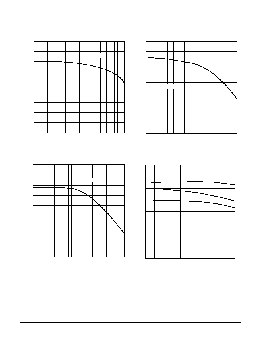
TYPICAL PERFORMANCE CHARACTERISTICS
1
10
100
34
36
38
40
42
44
46
48
50
52
Signal-to-Noise Ratio (dB)
Input Frequency (MHz)
S
= 125 MSPS
1
10
100
34
36
38
40
42
44
46
48
50
52
T
o
tal Har
monic Distor
tion (dB)
Input Frequency (MHz)
S
= 125 MSPS
1
10
100
34
36
38
40
42
44
46
48
50
52
Signal-to-Noise
and
Distortion
(dB)
Input Frequency (MHz)
S
= 125 MSPS
Temperature (∞C)
40
20
0
20
40
60
80
30
35
40
45
50
SNR, THD, SINAD (dB)
S
= 125 MSPS
IN
= 50 MHz
SNR
THD
SINAD
SNR vs Input Frequency
THD vs Input Frequency
SINAD vs Input Frequency
SNR, THD, SINAD vs Temperature
5
8/17/01
SPT7710
Figure 1 ≠ Typical Interface Circuit 1
Analog Input
Can Be Either
Force Or Sense
127
2
1
Preamp
Comparator
151
152
63
64
ECL
Latches
And
Buffers
VR2
V
RTF
LINV
MINV
2
D1
D2
D3
D4
D5
D6
MSB D7
LSB D0
2 V (Digital)
50 W
50 W
AGND
.01 µF
V
EE
5.2 V
L
Clock
Buffer
+
U1
5.2 V
V
EE
AGND
.01 µF
.01 µF
DGND
.01 µF
255
256
V
RBF
CLK
CLK
Convert
100116
50
W
50
W
V
IN
V
IN
256 To
8-Bit
Encoder
.01 µF
2 V
(Analog)
2.2 µF
Voltage
Limiter
*See below
Analog Input
Can Be Either
Force Or Sense
+
U2
.01 µF
V
EE
.01 µF
2.2 µF
2.2
2 V
VRef
10
V
EE
Q1 (1N2907A)
D1=D2=HP, 1N 5712
5.2
D1
D2
RS
49.9
Typical Voltage Limiter
R
T
128
GENERAL DESCRIPTION
The SPT7710 is a fast monolithic 8-bit parallel flash A/D
converter. The nominal conversion rate is 150 MSPS and
the analog bandwidth is in excess of 200 MHz. A major
advance over previous flash converters is the inclusion of
256 input preamplifiers between the reference ladder and
input comparators. (See block diagram.) This not only re-
duces clock transient kickback to the input and reference
ladder due to a low AC beta but also reduces the effect of
the dynamic state of the input signal on the latching char-
acteristics of the input comparators. The preamplifiers act
as buffers and stabilize the input capacitance so that it re-
mains constant for varying input voltages and frequencies
and, therefore, makes the part easier to drive than previ-
ous flash converters. The SPT7710 incorporates a propri-
etary decoding scheme that reduces metastable errors
(sparkle codes or
flyers) to a maximum of 1 LSB.
The SPT7710 has true differential analog and digital data
paths from the preamplifiers to the output buffers (Current
Mode Logic) for reducing potential missing codes while
rejecting common mode noise.
Signature errors are also reduced by careful layout of the
analog circuitry. Every comparator also has a clock buffer
to reduce differential delays and to improve signal-to-
noise ratio. The output drive capability of the device can
provide full ECL swings into 50
loads.
TYPICAL INTERFACE CIRCUIT
The typical interface circuit is shown in figure 1. The
SPT7710 is relatively easy to apply depending on the
accuracy needed in the intended application. Wire-wrap
may be employed with careful point-to-point ground con-
nections if desired, but to achieve the best operation, a