 | ÐлекÑÑоннÑй компоненÑ: SPT7721 | СкаÑаÑÑ:  PDF PDF  ZIP ZIP |
Äîêóìåíòàöèÿ è îïèñàíèÿ www.docs.chipfind.ru
SPT7721
8-BIT, 250 MSPS ADC WITH DEMUXED OUTPUTS
TECHNICAL DATA
NOVEMBER 8, 2001
GENERAL DESCRIPTION
The SPT7721 is a high-speed, 8-bit analog-to-digital con-
verter implemented in an advanced BiCMOS process. An
advanced folding and interpolating architecture provides
both a high conversion rate and very low power dissipation
of only 310 mW. The analog inputs can be operated in
either single-ended or differential input mode. A 2.5 V com-
mon mode reference is provided on chip for the single-
ended input mode to minimize external components.
The SPT7721 digital outputs are demuxed (double-wide)
with both dual-channel and single-channel selectable out-
put modes. Demuxed mode supports either parallel
aligned or interleaved data output. The output logic is both
+3.0 V and +5.0 V compatible. The SPT7721 is available in
a 44-lead TQFP surface mount package over the industrial
temperature range of 40 to +85 °C.
APPLICATIONS
· RGB video processing
· Digital communications
· High-speed instrumentation
· Projection display systems
FEATURES
· TTL/CMOS/PECL compatible
· High conversion rate: 250 MSPS
· Single +5 V power supply
· Very low power dissipation: 310 mW
· Power-down mode
· +3.0 V/+5.0 V (LVCMOS) digital output logic
compatibility
· Demuxed output ports
8-Bit
250 MSPS
ADC
CLK CLK
DB
0
DB
7
Common Mode
Voltage
Reference
+2.5 V
V
CM
AV
CC
OV
DD
AGND
DGND
DA
0
DA
7
PD
CLK CLK Reset
&
V
IN
+
Data Output Latches
V
IN
DCLK
OUT
DCLK
OUT
Data Output
Mode Control
DMODE
1,2
2
2
Reset
BLOCK DIAGRAM
2
11/8/01
SPT7721
ELECTRICAL SPECIFICATIONS
T
A
= T
MIN
to T
MAX
, AV
CC
= +5.0 V,
CLK
= 250 MHz, V
CM
= 2.5 V, OV
DD
= 5.0 V, unless otherwise specified.
TEST
TEST
SPT7721
PARAMETERS
CONDITIONS
LEVEL
MIN
TYP
MAX
UNITS
Resolution
8
Bits
DC Performance
IN
= 1 kHz
Differential Linearity Error (DLE)
+25 °C
V
0.70/+1.05
LSB
40 °C to +85 °C
V
0.95/+1.5
LSB
Integral Linearity Error (ILE)
+25 °C
V
±1.7
LSB
Best Fit
40 °C to +85 °C
V
±2.25
LSB
No Missing Codes
+25 °C,
IN
= 1 kHz
I
Guaranteed
Analog Input
Input Voltage Range
(with respect to V
IN
)
+25 °C
V
±470
mV
P-P
Gain Variation
VI
2
%
Input Common Mode (V
CM
)
IV
2.3
2.5
3.0
V
Input Bias Current
VI
10
µA
Input Resistance
+25 °C
V
50
k
Input Capacitance
+25 °C
V
4
pF
Input Bandwidth
+25 °C (3 dB of FS)
V
220
MHz
Offset Error
VI
±10
mV
Offset Power Supply Rejection Ratio
V
0.5
mV/V
Timing Characteristics
Maximum Conversion Rate
VI
250
MSPS
Output Delay (Clock-to-Data) (t
pd1
)
40 °C to +85 °C
IV
6
8
10.5
ns
Output Delay Tempco
V
22
ps/°C
Aperture Delay Time (t
ap
)
IV
0.5
ns
Aperture Jitter Time
IV
2
ps rms
Pipeline Delay (Latency)
Single Channel Mode
V
2.5
Clocks
Demuxed Interleaved Mode
V
2.5
Clocks
Demuxed Parallel Mode
Channel B
V
2.5
Clocks
Channel A
V
3.5
Clocks
CLK to DCLK
OUT
Delay Time
Single Channel Mode (t
pd2
)
IV
4
6
7
ns
Dual Channel Mode (t
pd3
)
IV
5.3
6.16
7.8
ns
Dynamic Performance
Effective Number of Bits (ENOB)
IN
= 70 MHz
+25 °C
VI
5.8
6.4
Bits
IN
= 70 MHz
40 °C to +85 °C
IV
5.5
6.0
Bits
Signal-to-Noise Ratio (SNR)
IN
= 70 MHz
+25 °C
VI
42
43
dB
IN
= 70 MHz
40 °C to +85 °C
IV
36
40
dB
Temperatures
Operating Temperature ........................... 40 to +85 °C
Storage Temperature ............................ 65 to +125 °C
Supply Voltages
AV
CC
...................................................................... +6 V
OV
DD
..................................................................... +6 V
Input Voltages
Analog Inputs ............................... 0.5 V to V
CC
+0.5 V
Digital Inputs ................................ 0.5 V to V
CC
+0.5 V
Note: Operation at any Absolute Maximum Rating is not implied.
See Electrical Specifications for proper applied conditions in
typical applications.
ABSOLUTE MAXIMUM RATINGS (Beyond which damage may occur) 25 °C

3
11/8/01
SPT7721
TEST LEVEL CODES
All electrical characteristics are subject to the
following conditions:
All parameters having min/max specifications
are guaranteed. The Test Level column indi-
cates the specific device testing actually per-
formed during production and Quality Assur-
ance inspection. Any blank section in the data
column indicates that the specification is not
tested at the specified condition.
ELECTRICAL SPECIFICATIONS
T
A
= T
MIN
to T
MAX
, AV
CC
= +5.0 V,
CLK
= 250 MHz, V
CM
= 2.5 V, OV
DD
= 5 V, unless otherwise specified.
TEST
TEST
SPT7721
PARAMETERS
CONDITIONS
LEVEL
MIN
TYP
MAX
UNITS
Dynamic Performance
Total Harmonic Distortion (THD)
IN
= 70 MHz
+25 °C
VI
43
40
dB
IN
= 70 MHz
40 °C to +85 °C
IV
42
37
dB
Signal-to-Noise and Distortion (SINAD)
IN
= 70 MHz
+25 °C
VI
37
40
dB
IN
= 70 MHz
40 °C to +85 °C
IV
35
38
dB
Power Supply Requirements
AV
CC
Voltage (Analog Supply)
IV
4.75
5.0
5.25
V
OV
DD
Voltage (Digital Supply)
IV
2.75
5.25
V
AV
CC
Current
VI
62
70
mA
Power Dissipation with Internal Voltage Reference
VI
310
350
mW
Common Mode Reference
Voltage
VI
2.45
2.5
2.55
V
Voltage Tempco
V
100
ppm/°C
Output Impedance
I
OUT
= ±50 µA
V
1
k
Power Supply Rejection Ratio
V
63
mV/V
Clock and Reset Inputs (Differential and Single-Ended)
Differential Signal Amplitude (V
DIFF)
VI
400
mV
P-P
Differential High Input Voltage (V
IHD)
IV
1.4
5
V
Differential Low Input Voltage (V
ILD)
IV
0
3.9
V
Differential Common-Mode Input (V
CMD)
IV
1.2
4.1
V
Single-Ended High Input Voltage (V
IH)
IV
1.8
V
Single-Ended Low Input Voltage (V
IL)
IV
1.2
V
Input Current High (II
H)
V
ID
= 1.5 V
VI
100
20
+100
µA
Input Current Low (II
L)
V
ID
= 1.5 V
VI
100
20
+100
µA
Power Down and Mode Control Inputs (Single-Ended)
High Input Voltage
IV
2.0
AV
CC
V
Low Input Voltage
IV
0
1.0
V
Maximum Input Current Low
VI
100
10
+100
µA
Maximum Input Current High <4.0 V
VI
100
10
+100
µA
Digital Outputs
Logic "1" Voltage
I
OH
= 0.5 mA
VI
OV
DD
0.2 OV
DD
0.06
V
Logic "0" Voltage
I
OL
= +1.6 mA
VI
0.13
0.2
V
T
R
/T
F
Data
10 pF load
OV
DD
= 3 V
V
3.5
ns
OV
DD
= 5 V
V
2.0
ns
T
R
/T
F
DCLK = (10 pF load)
OV
DD
= 3 V
V
1.3
ns
OV
DD
= 5 V
V
0.7
ns
LEVEL
TEST PROCEDURE
I
100% production tested at the specified temperature.
II
100% production tested at T
A
= +25 °C, and sample tested at the
specified temperatures.
III
QA sample tested only at the specified temperatures.
IV
Parameter is guaranteed (but not tested) by design and characteri-
zation data.
V
Parameter is a typical value for information purposes only.
VI
100% production tested at T
A
= +25 °C. Parameter is guaranteed
over specified temperature range.
4
11/8/01
SPT7721
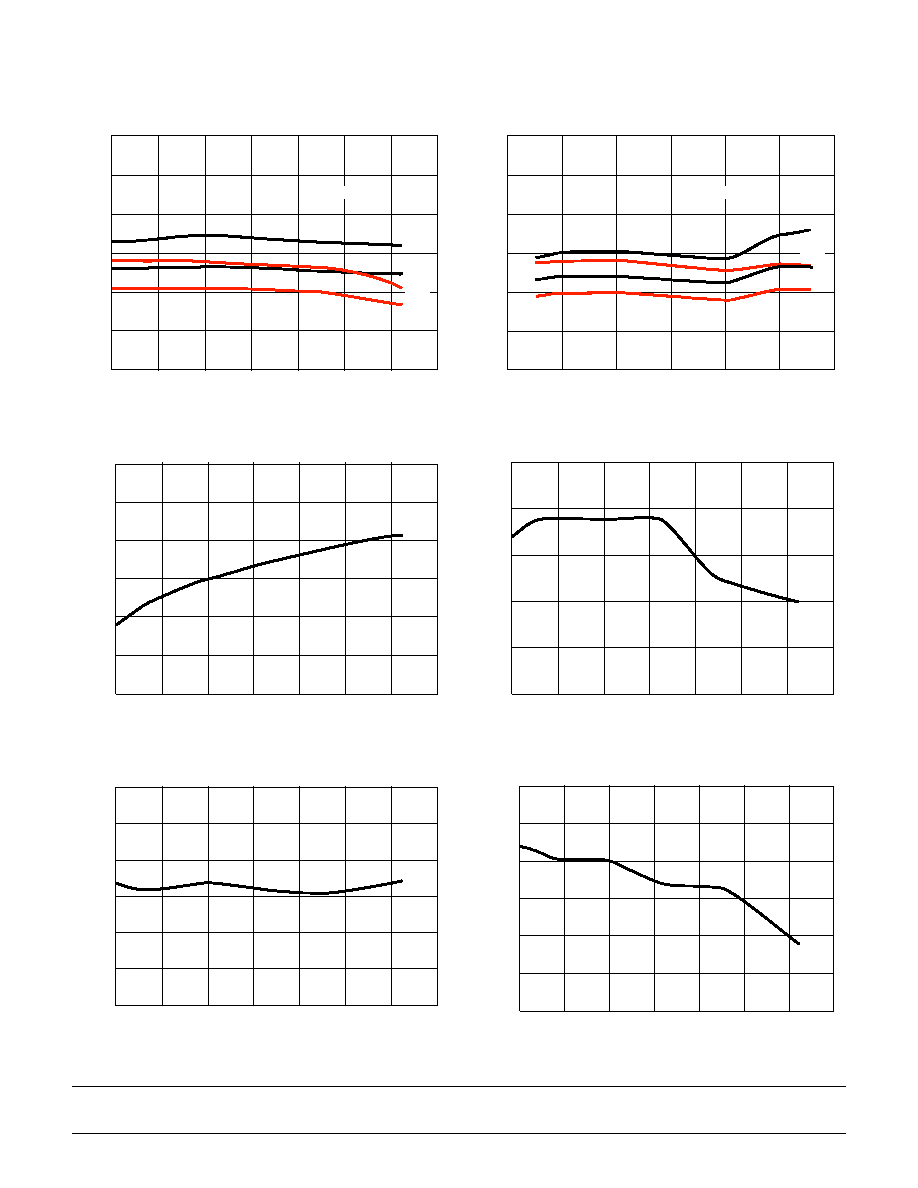
TYPICAL PERFORMANCE CHARACTERISTICS
AC Performance vs Temperature
40
20
0
20
40
60
80
35
40
45
50
55
60
Temperature (°C)
SFDR
THD
SNR
30
100
SFDR, THD, SNR, SINAD (dB)
SINAD
IN
= 70 MHz
0
35
40
45
50
55
60
Sample Rate (MSPS)
30
SFDR, SNR, THD, SINAD (dB)
50
100
150
200
250
300
SINAD
SNR
THD
SFDR
IN
= 70 MHz
AC Performance vs Sample Rate
AV
CC
Current vs Temperature
40
20
0
20
40
60
80
50
55
60
65
70
Temperature (°C)
45
100
AV
CC
(mA)
75
AV
CC
Current Power Down vs Temperature
40
20
0
20
40
60
80
2.2
2.4
2.6
2.8
3.0
Temperature (°C)
2.0
100
AV
CC
(mA)
Voltage Offset Error vs Temperature
Percent Gain Error vs Temperature
40
20
0
20
40
60
80
4.0
2.0
0.0
2.0
4.0
6.0
Temperature (°C)
6.0
100
mV
40
20
0
20
40
60
80
1.01
1.02
1.03
1.04
1.05
Temperature (°C)
1.00
100
%
1.06
5
11/8/01
SPT7721
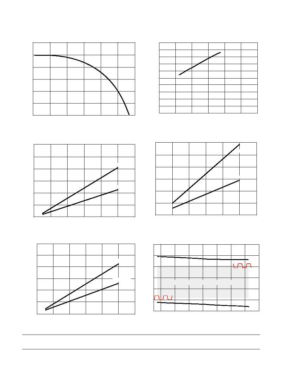
TYPICAL PERFORMANCE CHARACTERISTICS
Input Bandwidth
Common-Mode Reference Voltage vs V
CC
0
2
1
0
1
Input Frequency (MHz)
3
dB
100
200
300
400
500
600
4
5
4.5
2.42
2.45
2.48
2.50
V
CC
V
2.40
VCM
OUT
V
4.7
4.9
5.1
5.3
5.5
2.41
2.43
2.44
2.49
2.46
2.47
5.7
Total Power vs Clock Frequency
with 6 pF loads
0
400
500
600
700
800
300
50
100
150
200
250
300
Power Dissipation (mW)
Clock Frequency (MHz)
OV
DD
=5 V
1000
OV
DD
=3 V
OV
DD
Current vs Clock Frequency, Dual Mode
0
20
40
60
80
100
120
Clock Frequency (MHz)
0
mA
50
100
150
200
250
300
Output V
DD
=3 V
Output V
DD
=5 V
OV
DD
Current vs Clock Frequency, Single Mode
0
10
20
30
40
50
60
Clock Frequency (MHz)
0
mA
25
50
75
100
125
150
Output V
DD
=3 V
Output V
DD
=5 V
40
20
0
20
40
60
80
1
2
3
4
5
6
Temperature (°C)
0
100
V
olts
50
Common-Mode Operating Range
Differential Input Common-Mode Operating Range
400 mV
P-P