Äîêóìåíòàöèÿ è îïèñàíèÿ www.docs.chipfind.ru
Features
· TTL/CMOS/PECL input logic compatible
· High conversion rate: 250 MSPS
· Single +5V power supply
· Very low power dissipation: 425mW
· 350 MHz full power bandwidth
· Power-down mode: 24mW
· +3.0V/+5.0V (LVCMOS) digital output logic compatibility
· Single/demuxed output ports selectable
· Improved replacement for AD9054
Applications
· RGB video processing
· Digital communications
· High-speed instrumentation
· Digital Sampling Oscilloscopes (DSO)
· Projection display systems
Description
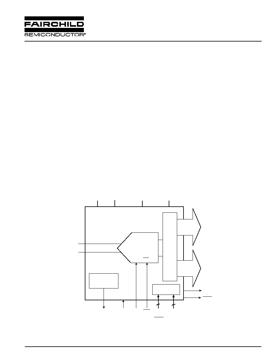
The SPT7722 is a high-speed, 8-bit analog-to-digital converter
implemented in an advanced BiCMOS process. It is a
performance-enhanced version of the SPT7721, offering
better linearity and dynamic performance. An advanced folding
and interpolating architecture provides both a high conversion
rate and very low power dissipation of only 425mW. The
analog inputs can be operated in either single-ended or
differential input mode. A 2.5V common mode reference is
provided on chip for the single-ended input mode to minimize
external components.
The SPT7722 digital outputs are demuxed (double-wide) with
both dual-channel and single-channel selectable output
modes. Demuxed mode supports either parallel aligned or
interleaved data output. The output logic is both +3.0V and
+5.0V compatible. The SPT7722 is available in a 44-lead
TQFP surface mount package over the industrial temperature
range of -40°C to +85°C.
SPT7722
8-bit, 250 MSPS A/D Converter with Demuxed Outputs
www.fairchildsemi.com
Rev. 1.0.2 December 2002
Block Diagram
8-Bit
250 MSPS
ADC
CLK CLK
DB
0
DB
7
Common Mode
Voltage
Reference
+2.5 V
V
CM
AV
CC
OV
DD
AGND
DGND
DA
0
DA
7
PD
CLK CLK Reset
&
V
IN
+
Data Output Latches
V
IN
DCLK
OUT
DCLK
OUT
Data Output
Mode Control
DMODE
1,2
2
2
Reset
DATA SHEET
SPT7722
2
Rev. 1.0.2 December 2002
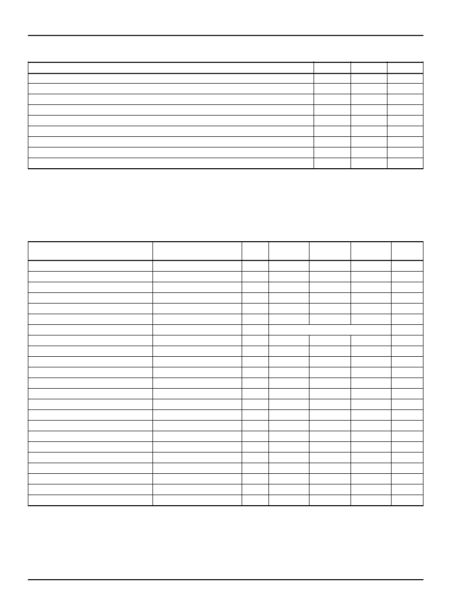
Absolute Maximum Ratings
(beyond which damage may occur)
1
25°C
Parameter
Min.
Max.
Unit
Supply Voltages
AV
CC
+6
V
OV
DD
+6
V
Input Voltages
Analog Inputs
-0.5
V
CC
+0.5
V
Digital Inputs
-0.5
V
CC
+0.5
V
Temperature
Operating Temperature
-40
+85
°C
Storage Temperature
-65
+125
°C
Note:
1. Operation at any absolute maximum rating is not implied.
See Electrical Specifications table for proper nominal applied conditions in typical applications.
Electrical Specifications
(T
A
= T
Min
to T
Max
, AV
CC
= +5V, OV
DD
= +5V,
clk
= 250MHz, 50% duty cycle,
IN
= 70MHz, dual channel mode; unless otherwise noted)
Parameter
Conditions
Test
Min.
Typ.
Max.
Unit
Level
Resolution
8
bits
DC Performance (IN = 1kHz)
Differential Linearity Error (DLE)
+25°C
VI
-0.68
±0.4
0.68
LSB
-40°C to +85°C
IV
-0.95
±0.7
0.95
LSB
Integral Linearity Error (ILE)
+25°C
VI
±1.2
±1.90
LSB
-40°C to +85°C
IV
±1.4
±2.15
LSB
No Missing Codes @250 MSPS
VI
Guaranteed
Analog Input
Input Voltage Range
with respect to V
IN
-
V
±512
mV
pp
Input Common Mode (V
CM
)
IV
2.0
2.5
3.0
V
Input Bias Current
+25°C
V
13
µA
Input Resistance
+25°C
V
50
k
Input Capacitance
+25°C
V
5
pF
Input Bandwidth
+25°C (3 dB of FS)
V
350
MHz
Gain Error
+25°C
VI
-7.5
+3.5
%FS
Offset Error
+25°C
VI
-5
+5
LSB
Offset Power Supply Rejection Ratio
AV
CC
= 5V ±0.25V
V
<1
LSB
Timing Characteristics
Conversion Rate
IV
25
250
MSPS
Output Delay (Clock-to-Data) (t
pd1
)
-40°C to +85°C
IV
7.0
8
9.4
ns
Output Delay Tempco
V
16
ps/°C
Aperture Delay Time (t
ap
)
V
0.3
ns
Aperture Jitter Time
V
2.0
ps-RMS
NOTE: All electrical characteristics are subject to the following condition:
All parameters having min/max specifications are guaranteed. The Test Level column indicates the specific devices testing actually performed
during production and quality assurance inspection. Any blank section in the data column indicates that the specification is not tested at the
specified condition.
SPT7722
DATA SHEET
Rev. 1.0.2 December 2002
3
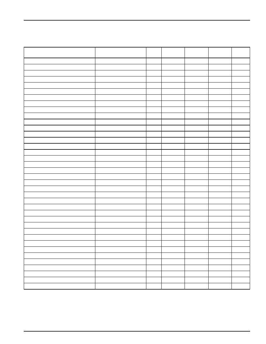
Electrical Specifications
(T
A
= T
Min
to T
Max
, AV
CC
= +5V, OV
DD
= +5V,
clk
= 250MHz, 50% duty cycle,
IN
= 70MHz, dual channel mode; unless otherwise noted)
Parameter
Conditions
Test
Min.
Typ.
Max.
Unit
Level
Pipeline Delay (Latency)
Single Channel Mode
V
2.5
Cycle
Demuxed Interleaved Mode
V
2.5
Cycle
Demuxed Parallel Mode
Channel B
V
2.5
Cycle
Channel A
V
3.5
Cycle
CLK to DCLK
OUT
Delay Time
Single Channel Mode (t
pd2
)
IV
5.0
5.18
5.3
ns
Dual Channel Mode (t
pd3
)
IV
5.6
5.73
5.9
ns
Output Delay (Clock to DClock)
V
18.1
ps/°C
Dynamic Performance
Effective Number of Bits (ENOB)
IN
= 70MHz
+25°C
VI
6.4
7.0
Bits
IN
= 70MHz
-40°C to +85°C
IV
6.25
6.8
Bits
Signal-to-Noise Ratio (SNR)
IN
= 70MHz
+25°C
VI
44.3
46.1
dB
IN
= 70MHz
-40°C to +85°C
IV
42.6
45.4
dB
Total Harmonic Distortion (THD)
IN
= 70MHz
+25°C
VI
-47
-41.5
dB
IN
= 70MHz
-40°C to +85°C
IV
-45.5
-40.3
dB
Signal-to-Noise & Distortion (SINAD)
IN
= 70MHz
+25°C
VI
40.2
43.7
dB
IN
= 70MHz
-40°C to +85°C
IV
39.3
42.8
dB
Power Supply Requirements
AV
CC
Voltage (Analog Supply)
IV
4.75
5.0
5.25
V
OV
DD
Voltage (Digital Supply)
IV
2.75
5.25
V
AV
CC
Current
VI
85
110
mA
AV
CC
Current Powerdown
+25°C
VI
4.8
5.5
mA
OV
DD
Current
OV
DD
= 3.0V, 10pF load
Single Mode
V
35
mA
Parallel Mode
V
55
mA
Interleave Mode
V
55
mA
Power Dissipation
VI
425
550
mW
Common Mode Reference Output
Voltage
VI
2.44
2.5
2.56
V
Voltage Tempco
V
84
ppm/°C
Output Impedance
I
OUT
= ±50
µ
A
V
1.07
k
Power Supply Rejection Ratio
V
47.5
mV/V
NOTE: All electrical characteristics are subject to the following condition:
All parameters having min/max specifications are guaranteed. The Test Level column indicates the specific devices testing actually performed
during production and quality assurance inspection. Any blank section in the data column indicates that the specification is not tested at the
specified condition.
DATA SHEET
SPT7722
4
Rev. 1.0.2 December 2002
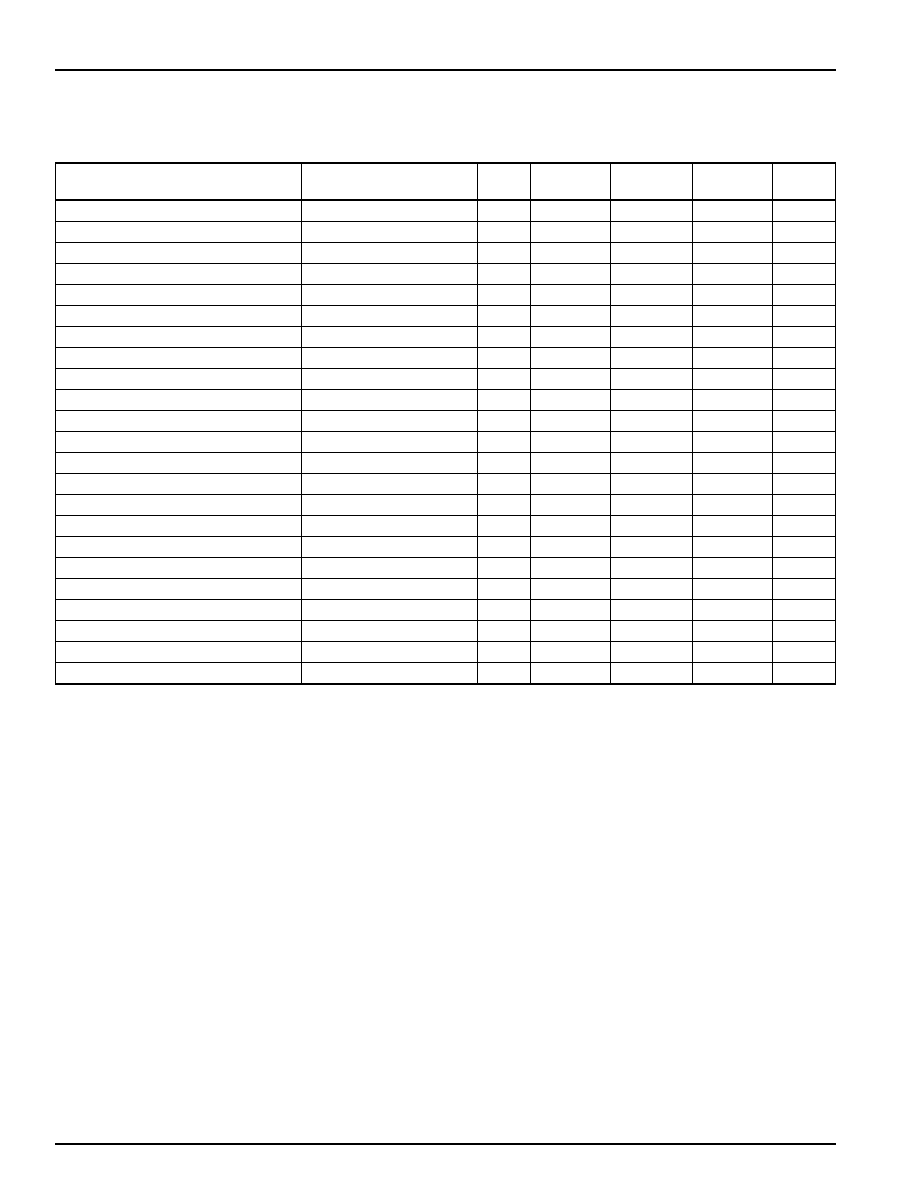
Electrical Specifications
(T
A
= T
Min
to T
Max
, AV
CC
= +5V, OV
DD
= +5V,
clk
= 250MHz, 50% duty cycle,
IN
= 70MHz, dual channel mode; unless otherwise noted)
Parameter
Conditions
Test
Min.
Typ.
Max.
Unit
Level
Clock and Reset Inputs
(Diff & Single-Ended)
Diff Signal Amplitude (V
DIFF
)
IV
400
mV
pp
Diff High Input Voltage (V
IHD
)
IV
1.4
AV
CC
V
Diff Low Input Voltage (V
ILD
)
IV
0
3.9
V
Diff Common Mode Input (V
CMD
)
IV
1.2
4.1
V
SE High Input Voltage (V
IH
)
IV
1.8
V
SE Low Input Voltage (V
IL
)
IV
0
1.2
V
Input Current High (I
IH
)
V
ID
= 1.5V
VI
100
43
+100
µ
A
Input Current Low (I
IL
)
V
ID
= 1.5V
VI
100
43
+100
µ
A
Power Down & Mode Control Inputs (Single-Ended)
High Input Voltage
IV
2.0
AV
CC
V
Low Input Voltage
IV
0
1.0
V
Max Input Current Low
VI
100
0.5
+100
µ
A
Max Input Current High <4.0V
VI
100
50
+100
µ
A
Digital Outputs
Logic "1" Voltage
I
OH
= -0.5mA
VI
OV
DD
-0.2
V
Logic "0" Voltage
I
OL
= +1.6mA
VI
0.2
V
T
R
/T
F
Data
10pF load
OV
DD
= 3V
V
3.3/3.0
ns
OV
DD
= 5V
V
2.3/1.9
ns
T
R
/T
F
DCLK
10pF load
OV
DD
= 3V
V
1.2/1.0
ns
OV
DD
= 5V
V
0.7/0.6
ns
NOTE: All electrical characteristics are subject to the following condition:
All parameters having min/max specifications are guaranteed. The Test Level column indicates the specific devices testing actually performed
during production and quality assurance inspection. Any blank section in the data column indicates that the specification is not tested at the
specified condition.
TEST LEVEL CODES:
Level
Test Procedure
I
100% production tested at the specified temperature.
II
100% production tested at T
A
= +25°C and sample tested at the specified temperatures.
II
QA sample tested only at the specified temperatures.
IV
Parameter is guaranteed (but not tested) by design and characterization data.
V
Parameter is a typical value for information purposes only.
VI
100% production tested at T
A
= +25°C. Parameter is guaranteed over specific temperature range.
SPT7722
DATA SHEET
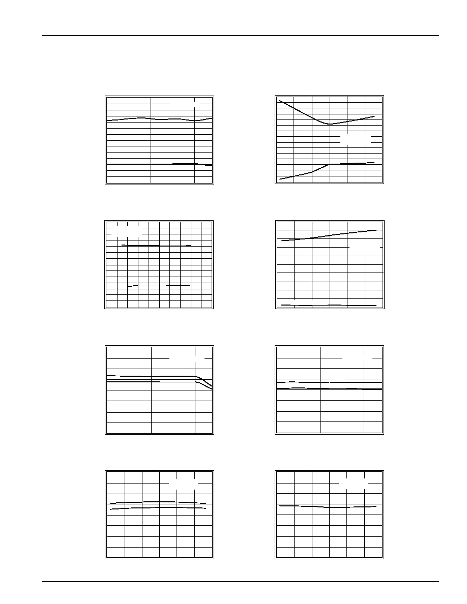
Typical Operating Characteristics
(T
A
= T
Min
to T
Max
, AV
CC
= +5V, OV
DD
= +5V,
clk
= 250MHz, 50% duty cycle,
IN
= 70MHz, dual channel mode; unless otherwise noted)
DLE vs. Sample Rate
0.7
0.1
0.0
-0.2
-0.5
LSB
-0.3
-0.4
-0.6
-0.7
-0.1
0.2
0.3
0.4
0.5
0.6
200
225
250
260
Sample Rate (MSPS)
IN
= 70.1 MHz
DLE vs. Temperature
-50
-25
25
75
100
0.8
0.1
0.0
-0.2
-0.5
Temperature (°C)
LSB
0
50
-0.3
-0.4
-0.6
-0.7
-0.1
0.2
0.3
0.4
0.5
0.6
0.7
IN
= 70.1MHz
S
= 250 MSPS
DLE vs. AV
CC
4.5
4.7
5.0 5.1
5.3
5.5
0.7
0.1
0.0
-0.2
-0.5
Volts
LSB
4.9
4.6
4.8
5.2
5.4
-0.3
-0.4
-0.6
-0.7
-0.1
0.2
0.3
0.4
0.5
0.6
IN
= 70.1MHz
S
= 250 MSPS
AV
CC
Current vs. Temperature
-50
-25
0
50
100
100
80
60
0
Temperature (°C)
AV
CC
Current (mA)
25
75
50
40
30
20
10
70
90
Powerdown mode
IN
= 70.1MHz
S
= 250 MSPS
SNR, SINAD vs. Sample Rate
200
225
250
260
Sample Rate (MSPS)
60
50
40
30
20
SNR, SINAD (dB)
55
45
35
25
SINAD
SNR
IN
= 70.1 MHz
SFDR, THD vs. Sample Rate
200
225
250
260
Sample Rate (MSPS)
-30
-40
-50
-60
-70
SFDR, THD (dB)
-35
-45
-55
-65
SFDR
THD
IN
= 70.1 MHz
SNR, SINAD vs. Temperature
60
50
40
30
20
Temperature (°C)
SNR, SINAD (dB)
SINAD
SNR
55
45
35
25
-50
-25
0
50
100
25
75
IN
= 70.1 MHz
S
= 250 MSPS
THD vs. Temperature
-30
-40
-50
-60
-70
Temperature (°C)
THD (dB)
-35
-45
-55
-65
-50
-25
0
50
100
25
75
IN
= 70.1 MHz
S
= 250 MSPS
Rev. 1.0.2 December 2002
5