SPT7725
8-BIT, 300 MSPS, FLASH A/D CONVERTER
TECHNICAL DATA
AUGUST 17, 2001
FEATURES
∑ Metastable errors reduced to 1 LSB
∑ Low input capacitance: 10 pF
∑ Wide input bandwidth: 210 MHz
∑ 300 MSPS conversion rate
∑ Typical power dissipation: 2.2 watts
APPLICATIONS
∑ Digital oscilloscopes
∑ Transient capture
∑ Radar, EW, ECM
∑ Direct RF down-conversion
∑ Medical electronics: ultrasound, CAT instrumentation
GENERAL DESCRIPTION
The SPT7725 is a monolithic flash A/D converter capable
of digitizing a two volt analog input signal into 8-bit digital
words at a 300 MSPS (typ) update rate.
For most applications, no external sample-and-hold is re-
quired for accurate conversion due to the device's narrow
aperture time, wide bandwidth, and low input capacitance.
A single standard ≠5.2 volt power supply is required for
operation of the SPT7725, with nominal power dissipation
of 2.2 W. A proprietary decoding scheme reduces meta-
stable errors to the 1 LSB level.
The SPT7725 is available in 42-lead ceramic sidebrazed
DIP, surface-mount 44-lead cerquad, and 46-lead PGA
packages (all are pin-compatible with the SPT7710); the
cerquad and PGA packages allow access to additional
reference ladder taps, an overrange bit, and a data ready
output. The SPT7725 is available in the industrial tem-
perature range.
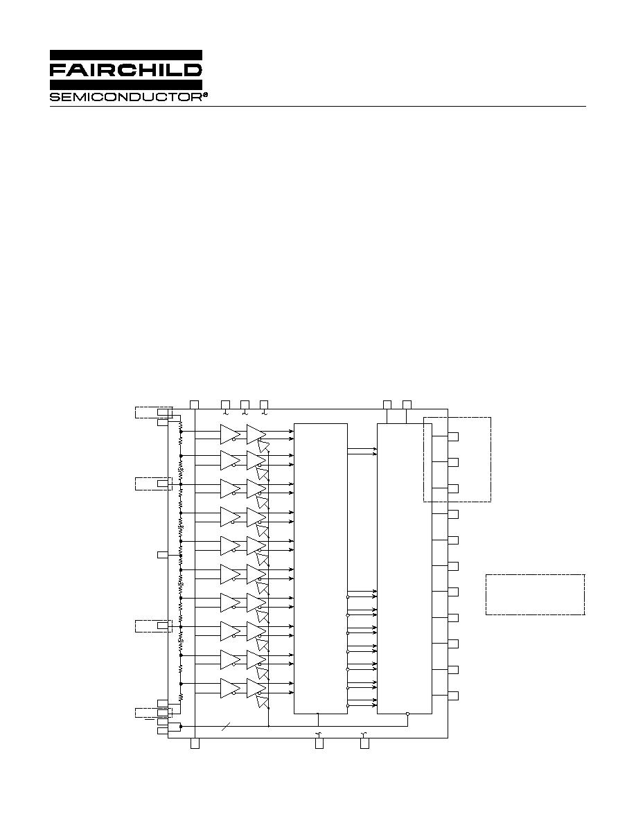
256
255
152
151
128
127
64
63
2
1
256 to
8-Bit
Encoder
ECL
Latches
and
Buffers
AGND
Analog Input
(Sense or Force)
VEE
CLK
CLK
V
RBF
Convert
V
RBS
V
R1
V
R3
V
RTS
V
RTF
V
R2
2
Analog Input
(Force or Sense) AGND DGND
V
EE
LINV MINV
DRINV
DREAD
Overrange
D7 MSB
D6
D5
D4
D3
D2
D1
D0 LSB
MSB D7
D6
D5
D4
D3
D2
D1
LSB D0
These functions are
available in the PGA and
cerquad packages only.
Clock
Buffer
Preamp
Comparator
BLOCK DIAGRAM

2
8/17/01
SPT7725
ABSOLUTE MAXIMUM RATINGS (Beyond which damage may occur)
1
25 ∞C
Note: 1. Operation at any Absolute Maximum Rating is not implied. See
Electrical Specifications for proper nominal applied conditions
in typical applications.
Supply Voltages
Negative Supply Voltage (V
EE
TO GND) ≠7.0 to +0.5 V
Ground Voltage Differential .................... ≠0.5 to +0.5 V
Input Voltage
Analog Input Voltage ............................... V
EE
to +0.5 V
Reference Input Voltage .......................... V
EE
to +0.5 V
Digital Input Voltage ................................ V
EE
to +0.5 V
Reference Current V
RTF
to V
RBF
........................ 25 mA
Output
Digital Output Current ............................... 0 to ≠30 mA
Temperature
Operating Temperature,ambient ............. ≠25 to +85 ∞C
junction ...................... +150 ∞C
Lead Temperature, (soldering 10 seconds) ..... +300 ∞C
Storage Temperature ............................ ≠65 to +150 ∞C
ELECTRICAL SPECIFICATIONS
T
A
= T
MIN
to T
MAX
, V
EE
=≠5.2 V, R
Source
=50
, V
RBF
=≠2.00 V, V
R2
=≠1.00 V, V
RTF
=0.00 V,
CLK
=250 MHz, Duty Cycle=50%, unless otherwise specified.
TEST
TEST
SPT7725A
SPT7725B
PARAMETERS
CONDITIONS
LEVEL
MIN
TYP
MAX
MIN
TYP
MAX
UNITS
DC Accuracy
Integral Linearity Error
CLK
= 100 kHz
VI
≠0.75
±0.60
+0.75
≠0.95
±0.80
+0.95
LSB
Differential Linearity Error
CLK
= 100 kHz
VI
≠0.75
+0.75
≠0.95
+0.95
LSB
No missing codes
Guaranteed
Guaranteed
Analog Input
Offset Error V
RT
VI
≠30
+30
≠30
+30
mV
Offset Error V
RB
VI
≠30
+30
≠30
+30
mV
Input Voltage Range
VI
≠2.0
0.0
≠2.0
0.0
Volts
Input Capacitance
Over full
input range
V
10
10
pF
Input Resistance
V
15
15
k
Input Current
VI
250
500
250
500
µA
Input Slew Rate
V
1,000
1,000
V/µs
Large Signal Bandwidth
V
IN
=F.S.
V
210
210
MHz
Small Signal Bandwidth
V
IN
=500 mV
P-P
V
335
335
MHz
Clock Synchronous
Input Currents
V
40
40
µA
Reference Input
Ladder Resistance
VI
100
200
300
100
200
300
Reference Bandwidth
V
10
10
MHz
Timing Characteristics
Maximum Sample Rate
IV
250
300
250
300
MSPS
Clock to Data Delay
V
2.4
2.4
ns
Output Delay Tempco
V
2
2
ps/∞C
CLK-to-Data Ready Delay (t
D
)
V
2.0
2.0
ns
Aperture Jitter
V
5
5
ps
Acquisition Time
V
1.5
1.5
ns
Dynamic Performance
Signal-to-Noise Ratio
IN
= 3.58 MHz
VI
45
47
44
46
dB
IN
= 50 MHz
VI
39
42
38
41
dB
Total Harmonic Distortion
IN
= 3.58 MHz
VI
≠52
≠48
≠50
≠46
dB
IN
= 50 MHz
VI
≠43
≠40
≠42
≠39
dB
Signal-to-Noise and Distortion
IN
= 3.58 MHz
VI
44
46
42
44
dB
(SINAD)
IN
= 50 MHz
VI
37
39
35
37
dB

3
8/17/01
SPT7725
TEST LEVEL CODES
All electrical characteristics are subject to the
following conditions:
All parameters having min/max specifications
are guaranteed. The Test Level column indi-
cates the specific device testing actually per-
formed during production and Quality Assur-
ance inspection. Any blank section in the data
column indicates that the specification is not
tested at the specified condition.
Unless otherwise noted, all test are pulsed
tests; therefore, T
J
= T
C
= T
A
.
LEVEL
TEST PROCEDURE
I
100% production tested at the specified temperature.
II
100% production tested at T
A
= +25 ∞C, and sample tested at the
specified temperatures.
III
QA sample tested only at the specified temperatures.
IV
Parameter is guaranteed (but not tested) by design and characteri-
zation data.
V
Parameter is a typical value for information purposes only.
VI
100% production tested at T
A
= +25 ∞C. Parameter is guaranteed
over specified temperature range.
ELECTRICAL SPECIFICATIONS
T
A
= T
MIN
to T
MAX
, V
EE
=≠5.2 V, R
Source
=50
, V
RBF
=≠2.00 V, V
R2
=≠1.00 V, V
RTF
=0.00 V,
CLK
=250 MHz, Duty Cycle=50%, unless otherwise specified.
TEST
TEST
SPT7725A
SPT7725B
PARAMETERS
CONDITIONS
LEVEL
MIN
TYP
MAX
MIN
TYP
MAX
UNITS
Digital Inputs
Digital Input High Voltage
(MINV, LINV)
VI
≠1.1
≠0.7
≠1.1
≠0.7
Volts
Digital Input Low Voltage
(MINV, LINV)
VI
≠2.0
≠1.5
≠2.0
≠1.5
Volts
Clock Low Width, t
PWL
VI
2.2
2.0
2
1.8
ns
Clock High Width, t
PWH
VI
2.2
2.0
2
1.8
ns
Digital Outputs
Digital Output High Voltage
50
to ≠2 V
VI
≠1.1
≠1.1
Volts
Digital Output Low Voltage
50
to ≠2 V
VI
≠1.5
≠1.5
Volts
Power Supply Requirements
Supply Current
+25 ∞C
VI
425
550
425
550
mA
Power Dissipation
+25 ∞C
VI
2.2
2.9
2.2
2.9
W
4
8/17/01
SPT7725
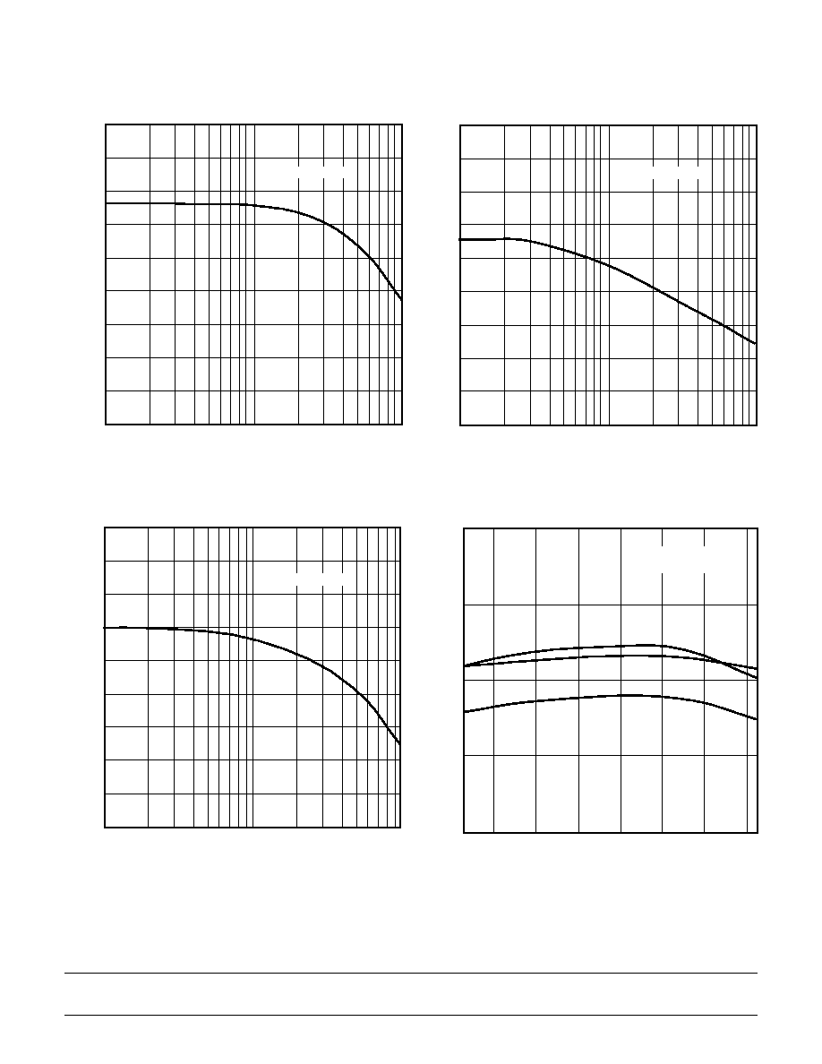
TYPICAL PERFORMANCE CHARACTERISTICS
SNR vs Input Frequency
THD vs Input Frequency
SINAD vs Input Frequency
SNR, THD, SINAD vs Temperature
1
10
100
34
36
38
40
42
44
46
48
50
52
Input Frequency (MHz)
S
= 250 MSPS
Signal-to-Noise
Ratio
(dB)
1
10
100
30
35
40
45
50
55
60
65
70
75
Input Frequency (MHz)
S
= 250 MSPS
T
o
tal
Harmonic
Distortion
(dB)
1
10
100
34
36
38
40
42
44
46
48
50
52
Input Frequency (MHz)
S
= 250 MSPS
Signal-to-Noise
and
Distortion
(dB)
Temperature (∞C)
40
20
0
20
40
60
80
30
35
40
45
50
SNR
THD
SINAD
S
= 250 MSPS
IN
= 100 MHz
SNR, THD, SINAD (dB)
5
8/17/01
SPT7725
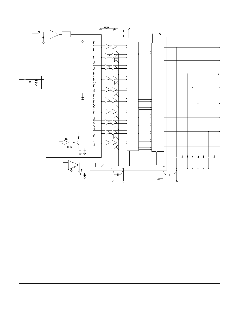
Figure 1 ≠ Typical Interface Circuit 1
Analog Input
Can Be Either
Force Or Sense
127
2
1
Preamp
Comparator
151
152
63
64
ECL
Latches
And
Buffers
VR2
V
RTF
LINV
MINV
2
D1
D2
D3
D4
D5
D6
MSB D7
LSB D0
2 V (Digital)
50 W
50 W
AGND
.01 µF
V
EE
5.2 V
L
Clock
Buffer
+
U1
5.2 V
V
EE
AGND
.01 µF
.01 µF
DGND
.01 µF
255
256
V
RBF
CLK
CLK
Convert
100116
50
W
50
W
V
IN
V
IN
256 To
8-Bit
Encoder
.01 µF
2 V
(Analog)
2.2 µF
Voltage
Limiter
*See below
Analog Input
Can Be Either
Force Or Sense
+
U2
.01 µF
V
EE
.01 µF
2.2 µF
2.2
2 V
VRef
10
V
EE
Q1 (1N2907A)
D1=D2=HP, 1N 5712
5.2
D1
D2
RS
49.9
Typical Voltage Limiter
R
T
128
GENERAL DESCRIPTION
The SPT7725 is a fast monolithic 8-bit parallel flash A/D
converter. The nominal conversion rate is 300 MSPS and
the analog bandwidth is in excess of 200 MHz. A major ad-
vance over previous flash converters is the inclusion of
256 input preamplifiers between the reference ladder and
input comparators. (See block diagram.) This not only re-
duces clock transient kickback to the input and reference
ladder due to a low AC beta but also reduces the effect of
the dynamic state of the input signal on the latching char-
acteristics of the input comparators. The preamplifiers act
as buffers and stabilize the input capacitance so that it re-
mains constant for varying input voltages and frequencies
and, therefore, makes the part easier to drive than previ-
ous flash converters. The SPT7725 incorporates a propri-
etary decoding scheme that reduces metastable errors
(sparkle codes or
flyers) to a maximum of 1 LSB.
The SPT7725 has true differential analog and digital data
paths from the preamplifiers to the output buffers (Current
Mode Logic) for reducing potential missing codes while
rejecting common mode noise.
Signature errors are also reduced by careful layout of the
analog circuitry. Every comparator also has a clock buffer
to reduce differential delays and to improve signal-to-
noise ratio. The output drive capability of the device can
provide full ECL swings into 50
loads.
TYPICAL INTERFACE CIRCUIT
The typical interface circuit is shown in figure 1. The
SPT7725 is relatively easy to apply depending on the
accuracy needed in the intended application. Wire-wrap
may be employed with careful point-to-point ground con-
nections if desired, but to achieve the best operation, a
6
8/17/01
SPT7725
double-sided PC board with a ground plane on the compo-
nent side separated into digital and analog sections will
give the best performance. The converter is bonded-out to
place the digital pins on the left side of the package and
the analog pins on the right side. Additionally, an RF bead
connection through a single point from the analog to digi-
tal ground planes will reduce ground noise pickup.
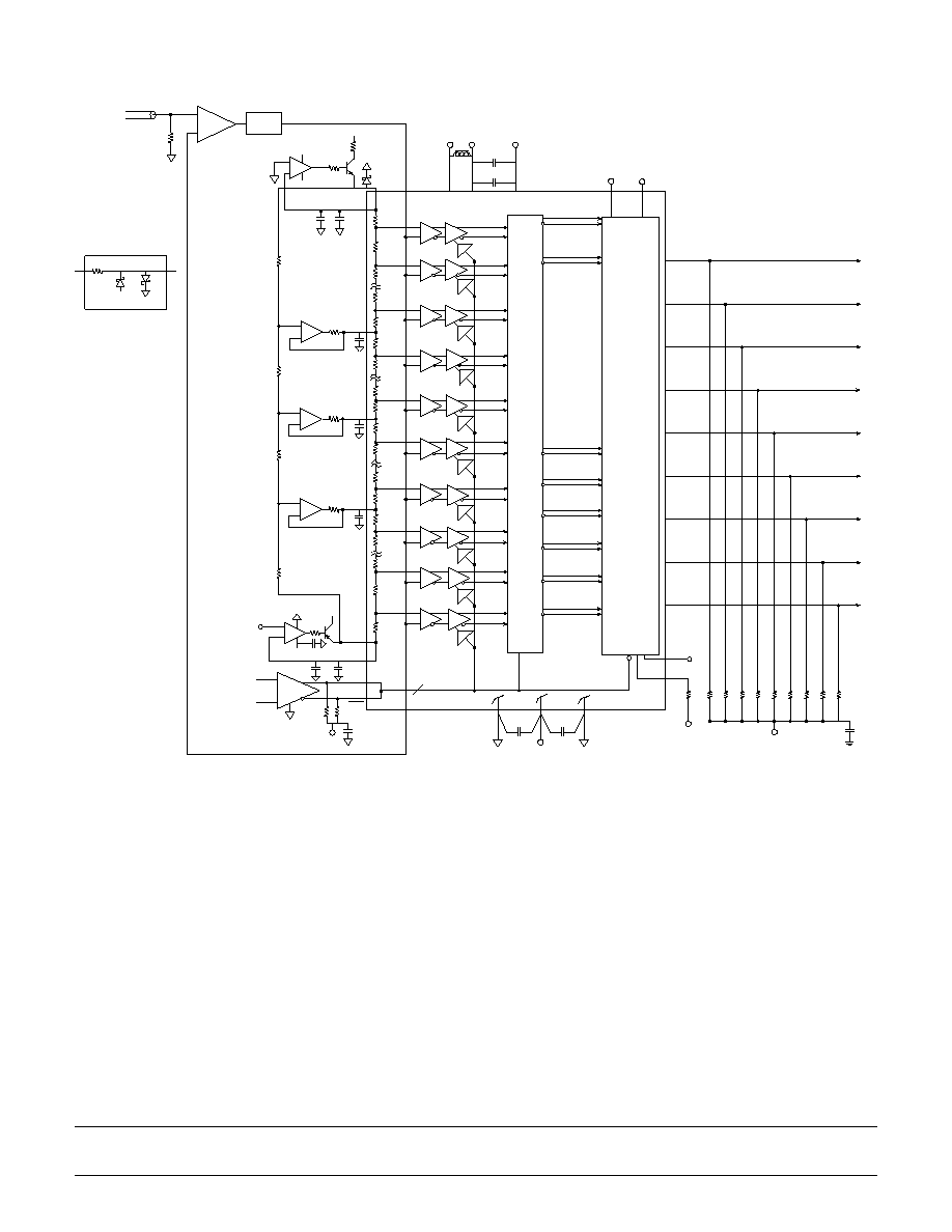
The circuit in figure 2 (PGA and cerquad packages only) is
intended to show the most elaborate method of achieving
the least error by correcting for integral nonlinearity, input
induced distortion, and power supply/ground noise. This is
achieved by the use of external reference ladder tap con-
nections, an input buffer, and supply decoupling. The func-
tion of each pin and external connections to other compo-
nents is as follows:
Figure 2 ≠ Typical Interface Circuit 2 (PGA and Cerquad packages only)
V
EE
V
CC
10-25 W
V
R1
+
.01 µF
256 to
8-Bit
Encoder
ECL
Latches
And
Buffers
V
R2
V
RTF
LINV
MINV
V
RBF
Analog
Input
Force
2 V
2.2 µF
5.2 V
Clock
Buffer
Preamp Comparator
V
EE
AGND
DGND
V
RTS
V
RBS
50 W
DREAD
DRINV
Overrange
D8
MSB
D7
D6
D5
D4
D3
D2
D1
LSB
D0
AGND
V
EE
AGND
5.2 V
.01 µF
.01 µF
2
Analog Input
(Sense)
.01 µF
CLK
CLK
100116
Convert
50
W
50
W
2 V (Digital)
L
10-25 W V
R3
+
.01 µF
10-25 W
+
.01 µF
V
IN
V
IN
50 W
2
128
64
191
256
127
192
151
63
1
.01 µF
2 V
(Analog)
V
EE
U2
U2
U2
U1 and U2=
Rail-to-Rail Op Amp
D1=HP, 1N5712
Q1=1N2222A
Q2=1N2907A
R = 1 kW, .1%
R
R
R
R
+
U1
Voltage
Limiter
*See below
R
T
5.2
D1
D2
RS
49.9
Typical Voltage Limiter
.01 µF
.01 µF
2.2 µF
+
U1
22
10 W
V
CC
Q1
D1
.01 µF
2.2 µF
V
EE
2 V
V
REF
V
EE
+
22 W
U2
.01 µF
V
EE
, AGND, DGND
V
EE
is the supply pin with AGND as ground for the device.
The power supply pins should be bypassed as close to the
device as possible with at least a .01 µF ceramic capaci-
tor. A 1 µF tantalum should also be used for low frequency
suppression. DGND is the ground for the ECL outputs and
is to be referenced to the output pulldown voltage and
appropriately bypassed as shown in figure 1.
V
IN
(ANALOG INPUT)
There are two analog input pins that are tied to the same
point internally. Either one may be used as an analog input
sense and the other for input force. This is convenient for
testing the source signal to see if there is sufficient drive
capability. The pins can also be tied together and driven by
7
8/17/01
SPT7725
the same source. The SPT7725 is superior to similar de-
vices, due to a preamplifier stage before the comparators.
This makes the device easier to drive because it has con-
stant capacitance and induces less slew rate distortion.
An optional input buffer may be used.
CLK,
CLK
(CLOCK INPUTS)
The clock inputs are designed to be driven differentially
with ECL levels. The clock may be driven single-ended
since
CLK
is internally biased to ≠1.3 V. (See clock input
circuit.)
CLK
may be left open, but a .01 µF bypass capaci-
tor from
CLK
to AGND is recommended. NOTE: System
performance may be degraded due to increased clock
noise or jitter.
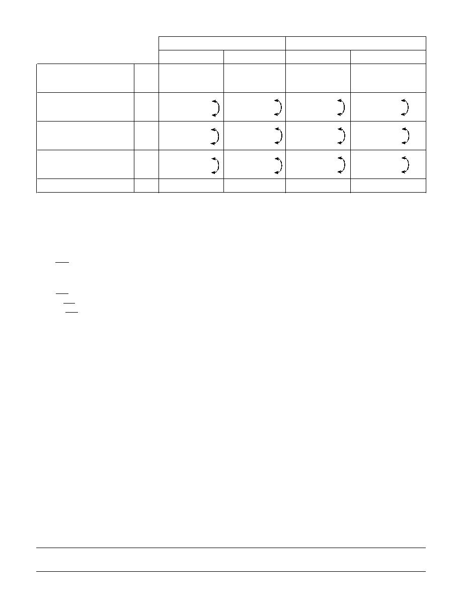
MINV, LINV (OUTPUT LOGIC CONTROL)
These are ECL-compatible digital controls for changing
the output code from straight binary to two's complement,
etc. For more information, see table I. Both MINV and
LINV are in the logic low (0) state when they are left open.
The high state can be obtained by tying to AGND through
a diode or 3.9 k
resistor.
D0 TO D7 (DIGITAL OUTPUTS)
The digital outputs can drive ECL levels into 50
when
pulled down to ≠2 V. When pulled down to ≠5.2 V, the out-
puts can drive 150
to 1 k
loads.
V
RBF
, V
R2
, V
RTF
(REFERENCE INPUTS)
There are two reference inputs and one external reference
voltage tap. These are ≠2 V (V
RBF
), mid-tap (V
R2
), and
AGND (V
RTF
). The reference pins can be driven as shown
in figure 1. V
R2
should be bypassed to AGND for further
noise suppression.
V
RBF
, V
RBS
, V
R1
, V
R2
, V
R3
, V
RTF
, V
RTS
REFERENCE
INPUTS
(PGA AND CERQUAD PACKAGES ONLY)
These are five external reference voltage taps from ≠2 V
(V
RBF
) to AGND (V
RTF
) that can be used to control integral
linearity over temperature. The taps can be driven by op
amps as shown in figure 2. These voltage level inputs can
be bypassed to AGND for further noise suppression if so
desired. V
RB
and V
RT
have force and sense pins for moni-
toring the top and bottom voltage references.
N/C
All
Not Connected pins should be tied to DGND on the left
side of the package and to AGND on the right side of the
package.
DREAD ≠ DATA READY; DRINV ≠ DATA READY
INVERSE
(PGA AND CERQUAD PACKAGES ONLY)
The data ready pin is a flag that goes high or low at the
output when data is valid or ready to be received. It is es-
sentially a delay line that accounts for the time neces-
sary for information to be clocked through the SPT7725's
decoders and latches. This function is useful for interfac-
ing with high-speed memory. Using the data ready output
to latch the output data ensures minimum set-up and hold
times. DRINV is a data ready inverse control pin. (See the
timing diagram.)
D8 ≠ OVERRANGE
(PGA AND CERQUAD PACKAGES
ONLY)
This is an overrange function. When the SPT7725 is in an
overrange condition, D8 goes high and all data outputs go
high as well. This makes it possible to include the
SPT7725 into higher resolution systems.
BINARY
TWOs COMPLEMENT
TRUE
INVERTED
TRUE
INVERTED
MINV=LINV=0
MINV=LINV=1
MINV=1; LINV=0 MINV=0; LINV=1
ANALOG INPUT VOLTAGE
D8
D7_____D0
D7_____D0
D7_____D0
D7_____D0
≠2 V + 1/2 LSB
0
00000000
11111111
10000000
01111111
00000001
11111110
10000001
01111110
≠1.0 V
0
01111111
10000000
11111111
00000000
10000000
01111111
00000000
11111111
0 V ≠ 1/2 LSB
0
11111111
00000000
01111111
10000000
11111110
00000001
01111110
10000001
0 V
1
11111111
00000000
01111111
10000000
Table I ≠ Output Coding
8
8/17/01
SPT7725
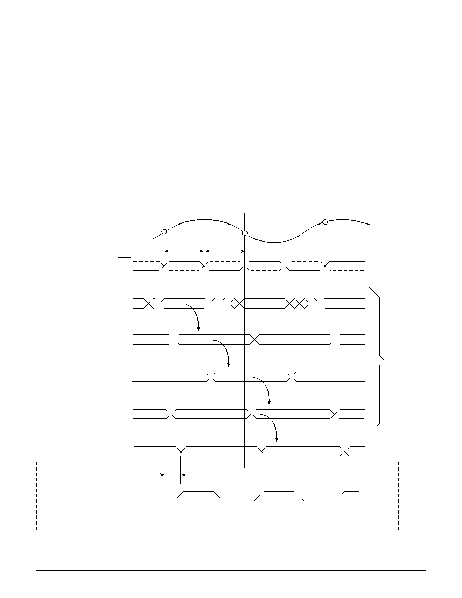
OPERATION
The SPT7725 has 256 preamp/comparator pairs that are
each supplied with the voltage from V
RTF
to V
RBF
divided
equally by the resistive ladder as shown in the block dia-
gram. This voltage is applied to the positive input of each
preamplifier/comparator pair. An analog input voltage ap-
plied at V
IN
is connected to the negative inputs of each
preamplifier/comparator pair. The comparators are then
clocked through each comparator's individual clock buffer.
When CLK pin is in the low state, the master or input stage
of the comparators compares the analog input voltage to
the respective reference voltage. When CLK changes
from low to high, the comparators are latched to the state
prior to the clock transition and output logic codes in
sequence from the top comparators, closest to V
RTF
(0 V),
down to the point where the magnitude of the input signal
changes sign (thermometer code). The output of each
comparator is then registered into four 64-to-6 bit decod-
ers when CLK is changed from high to low.
At the output of the decoders is a set of four 7-bit latches
that are enabled (
track) when CLK changes from high to
low. From here, the outputs of the latches are coded into
6 LSBs from 4 columns, and 4 columns are coded into
2 MSBs. Next are the MINV and LINV controls for output
inversions, which consist of a set of eight XOR gates.
Finally, 8 ECL output latches and buffers are used to drive
the external loads. The conversion takes one clock cycle
from the input to the data outputs.
Figure 3 ≠ Timing Diagram
t
PW1
N
N+2
N+1
N
N1
t
D
Data Output D0D7
CLK
Analog Input
Clock
V
IN
6 Bit Latch Output
8 Bit Latch Output
Master
Slave
CLK
Comparator Output
N+1
Data Ready
Overrange D8
Timing for PGA and Cerquad Packages Only
Internal T
iming
t
PW0
9
8/17/01
SPT7725
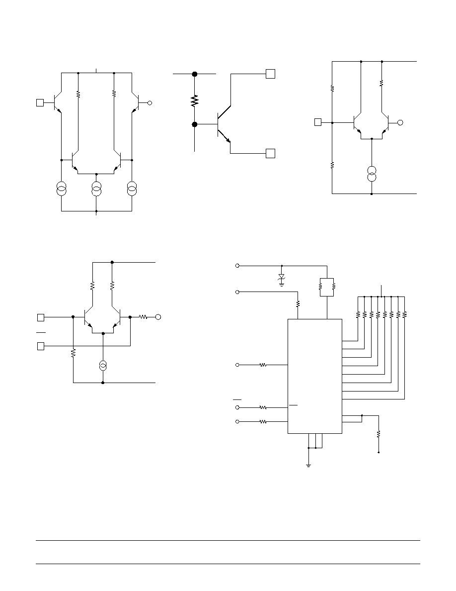
Figure 4 ≠ Subcircuit Schematics
AGND
V
IN
V
EE
V
R
Input Circuit
AGND
1.3 V
V
EE
MINV
LINV
10 kW
16 kW
MINV, LINV Input Circuit
Output Circuit
AGND
Data Out
DGND
Figure 5 ≠ Clock Input
AGND
1.3 V
13 kW
13 kW
V
EE
CLK
CLK
Figure 6 ≠ Burn-In Circuit (42-lead DIP Package only)
R2
R
1
= 50 W 1/4 Watt CC 5%
R
2
= 1 kW 1/4 Watt CC 5%
R
3
= 6.5 W 1/4 Watt CC 5%
R
4
= 6.5 W 1/2 Watt CC 5%
V
REF
= 2.0 Volts
V
EE
= 6.6 Volts
R3
V
RBF
V
EE
1N4736
R4
R4
LINV
MINV
R2
2.0 V
AGND
V
RT
F
DGND
R2
R2
V
IN
V
REF
V
EE
CLK
CLK
2.0 V
R1 R1
R1 R1 R1 R1 R1
R1
V
IN
D0
D1
D2
D3
D4
D5
D6
D7
CLK
CLK
EVALUATION BOARDS
The EB7725 evaluation board is available to aid designers
in demonstrating the full performance of the SPT7725.
This board includes a voltage reference circuit, clock
driver circuit, output data latches, and an on-board recon-
struction of the digital data. An application note describing
the operation of this board, as well as application tips, is
also available. Contact the factory for price and delivery.
10
8/17/01
SPT7725
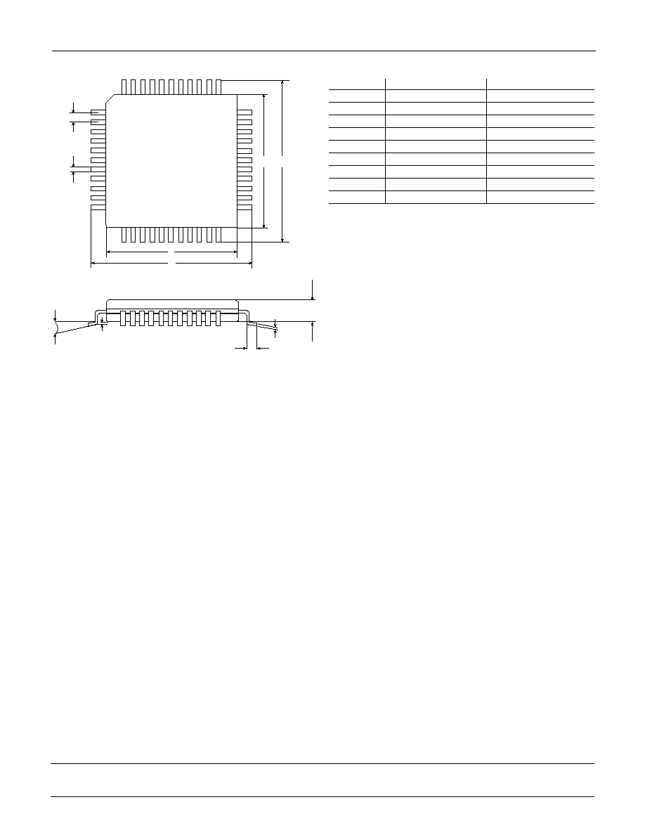
PACKAGE OUTLINES
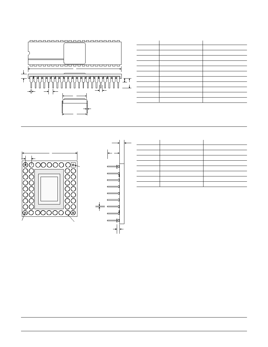
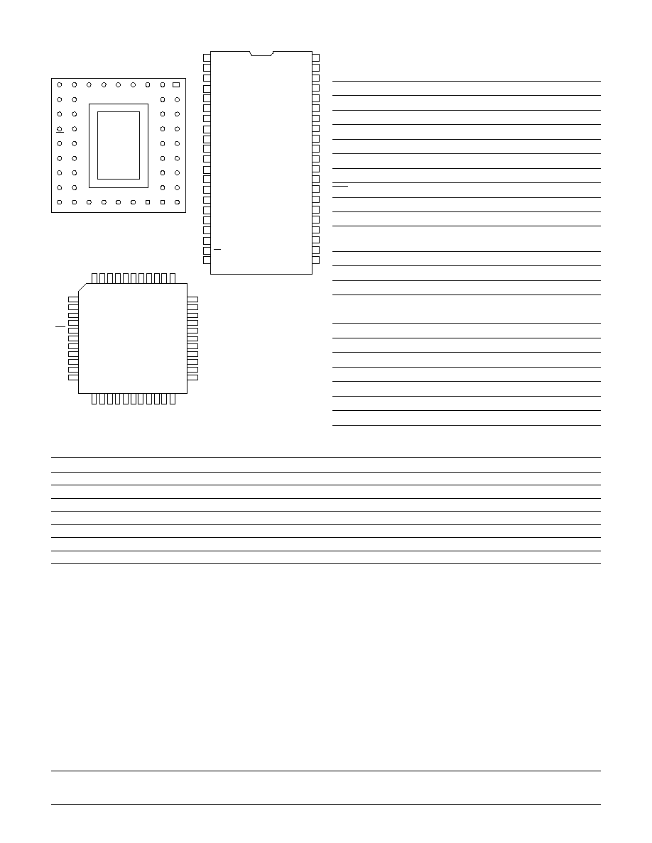
42-Lead Sidebrazed DIP
A
B
C
D
E
G
1
42
I
H
J
F
46-Lead Pin Grid Array
A
B
C Diameter
Pin 1
D
E
F
G
Stand-off Pin
INCHES
MILLIMETERS
SYMBOL
MIN
MAX
MIN
MAX
A
0.081
0.099
2.06
2.51
B
0.016
0.020
0.41
0.51
C
0.095
0.105
2.41
2.67
D
.050 typ
1.27
E
.050 typ
1.27
F
0.275
6.99
G
2.080
2.120
52.83
53.85
H
0.585
0.605
14.86
15.37
I
0.008
0.015
0.20
0.38
J
0.600
0.620
15.24
15.75
INCHES
MILLIMETERS
SYMBOL
MIN
MAX
MIN
MAX
A
0.890
0.910
22.61
23.11
B
0.100 typ
2.54 typ
C
.045 dia
.055 dia
1.14
1.40
D
0.084
0.096
2.13
2.44
E
0.169
0.193
4.29
4.90
F
.020 dia
.030 dia
0.51
0.76
G
.050 typ
1.27 typ
11
8/17/01
SPT7725
44-Lead Cerquad
C
D
A
B
A
B
05∞
E
F
G
H
INCHES
MILLIMETERS
SYMBOL
MIN
MAX
MIN
MAX
A
0.550 typ
13.97 typ
B
0.685
0.709
17.40
18.00
C
0.037
0.041
0.94
1.04
D
0.016 typ
0.41 typ
E
0.008 typ
0.20 typ
F
0.027
0.051
0.69
1.30
G
0.006 typ
0.15 typ
H
0.080
0.089
2.03
2.26
12
8/17/01
SPT7725
AGND
V
EE
LINV
N/C
DRINV
N/C
V
EE
AGND
AGND
V
RTS
V
RTF
D8
D7
D6
D5
D4
D3
D2
D1
D0
DREADY
DGND
V
EE
V
R1
AGND
V
IN
AGND
V
R2
AGND
V
IN
AGND
V
R3
V
EE
DGND
AGND
V
EE
MINV
CLK
CLK
V
EE
AGND
AGND
V
RBS
V
RBF
1
2
3
4
5
6
7
8
9
10
11
33
32
31
30
29
28
27
26
25
24
23
12
13
14
15
16
17
18
19
20
21
22
44
43
42
41
40
39
38
37
36
35
34
Cerquad
ORDERING INFORMATION
PART NUMBER
LINEARITY
TEMPERATURE RANGE
PACKAGE TYPE
SPT7725AIJ
0.75 LSB
≠25 to +85 ∞C
42L Ceramic S/B
SPT7725BIJ
0.95 LSB
≠25 to +85 ∞C
42L Ceramic S/B
SPT7725AIG
0.75 LSB
≠25 to +85 ∞C
46L PGA
SPT7725BIG
0.95 LSB
≠25 to +85 ∞C
46L PGA
SPT7725AIQ
0.75 LSB
≠25 to +85 ∞C
44L Cerquad
SPT7725BIQ
0.95 LSB
≠25 to +85 ∞C
44L Cerquad
SPT7725BCU
0.95 LSB
+25 ∞C
Die*
*Please see the die specification for guaranteed electrical performance.
PIN ASSIGNMENTS
PIN FUNCTIONS
Name
Function
LINV
D0 through D6 Output Inversion Control Pin
V
EE
Negative Analog Supply Nominally ≠5.2 V
DGND
Digital Ground
D0
Digital Data Output (LSB)
D1≠D6
Digital Data Output
D7
Digital Data Output (MSB)
MINV
D7 Output Inversion Control Pin
CLK
Inverse ECL Clock Input Pin
CLK
ECL Clock Input Pin
AGND
Analog Ground
V
IN
Analog Input; Can be Connected to the
Input Signal or Used as a Sense
V
R2
Reference Voltage Tap 2 (≠1.0 V typ)
V
RTF
Reference Voltage Top
V
RBF
Reference Voltage Bottom
The following pins are on PGA and cerquad packages only.
DRINV
Data Ready Inverse
DREAD
Data Ready Output
Overrange Overrange Output D8
V
R1
Reference Voltage Tap 1 (≠1.5 V typ)
V
R3
Reference Voltage Tap 3 (≠0.5 V typ)
V
RTS
Reference Voltage Top, Sense
V
RBS
Reference Voltage Bottom, Sense
V
IN
V
EE
V
EE
V
EE
V
EE
1
2
4
3
5
6
7
8
9
10
11
12
13
14
15
16
17
18
19
20
21
22
23
24
25
26
27
28
29
30
31
32
33
34
35
36
37
38
39
40
41
42
N/C
LINV
AGND
DGND
D0 (LSB)
D1
D2
D3
D4
D5
D6
D7 (MSB)
DGND
AGND
V
EE
MINV
N/C
CLK
CLK
N/C
V
RTF
N/C
N/C
N/C
AGND
AGND
V
R2
AGND
AGND
N/C
N/C
V
EE
N/C
V
RBF
N/C
V
IN
V
EE
A
B
C
D
E
F
G
H
D8
D6
D5
D4
D3
D2
D1
D0
DGND
N/C
AGND
V
IN
AGND
V
R2
AGND
V
IN
AGND
N/C
VRBF
V
RBS
VR1
V
EE
V
R3
N/C
V
EE
V
RTF
AGND AGND
V
RTS
AGND
V
EE
CLK
V
EE
AGND
VEE DGND
N/C
V
EE
AGND
D7
AGND
DREAD
MINV
LINV DRINV
CLK
1
2
3
4
5
6
7
8
9
J
Bottom
View
PGA
DIP
LIFE SUPPORT POLICY
FAIRCHILD'S PRODUCTS ARE NOT AUTHORIZED FOR USE AS CRITICAL COMPONENTS IN LIFE SUPPORT DEVICES OR SYSTEMS
WITHOUT THE EXPRESS WRITTEN APPROVAL OF THE PRESIDENT OF FAIRCHILD SEMICONDUCTOR CORPORATION. As used herein:
1. Life support devices or systems are devices or systems which, (a) are
intended for surgical implant into the body, or (b) support or sustain life,
and whose failure to perform, when properly used in accordance with
instructions for use provided in the labeling, can be reasonably
expected to result in a significant injury to the user.
2. A critical component is any component of a life support device or
system whose failure to perform can be reasonably expected to cause
the failure of the life support device or system, or to affect its safety or
effectiveness.
DISCLAIMER
FAIRCHILD SEMICONDUCTOR RESERVES THE RIGHT TO MAKE CHANGES WITHOUT FURTHER NOTICE TO ANY PRODUCTS HEREIN TO
IMPROVE RELIABILITY, FUNCTION OR DESIGN. FAIRCHILD DOES NOT ASSUME ANY LIABILITY ARISING OUT OF THE APPLICATION OR
USE OF ANY PRODUCT OR CIRCUIT DESCRIBED HEREIN; NEITHER DOES IT CONVEY ANY LICENSE UNDER ITS PATENT RIGHTS, NOR
THE RIGHTS OF OTHERS.
www.fairchildsemi.com
© Copyright 2002 Fairchild Semiconductor Corporation