Äîêóìåíòàöèÿ è îïèñàíèÿ www.docs.chipfind.ru
SPT7734
8-BIT, 40 MSPS,175 mW A/D CONVERTER
FEATURES
· Monolithic 40 MSPS Converter
· 175 mW Power Dissipation
· On-Chip Track-and-Hold
· Single +5 V Power Supply
· TTL/CMOS Outputs
· 5 pF Input Capacitance
· Low Cost
· Tri-State Output Buffers
· High ESD Protection: 3,500 V Minimum
· Selectable +3 V or +5 V Logic I/O
APPLICATIONS
· All High-Speed Applications Where
Low Power Dissipation is Required
· Video Imaging
· Medical Imaging
· Radar Receivers
· IR Imaging
· Digital Communications
GENERAL DESCRIPTION
The SPT7734 is a 8-bit monolithic, low cost, ultralow power
analog-to-digital converter capable of minimum word rates
of 40 MSPS. The on-chip track-and-hold function assures
very good dynamic performance without the need for exter-
nal components. The input drive requirements are mini-
mized due to the SPT7734's low input capacitance of only
5 pF.
Power dissipation is extremely low at only 175 mW typical at
40 MSPS with a power supply of +5.0 V. The digital outputs
are +3 V or +5 V, and are user selectable. The SPT7734 has
incorporated proprietary circuit design and CMOS process-
ing technologies to achieve its advanced performance. In-
puts and outputs are TTL/CMOS compatible to interface with
TTL/CMOS logic systems. Output data format is straight
binary.
The SPT7734 is available in 28-lead SOIC and 32-lead small
(7 mm square) TQFP packages over the commercial tem-
perature range.
.
.
.
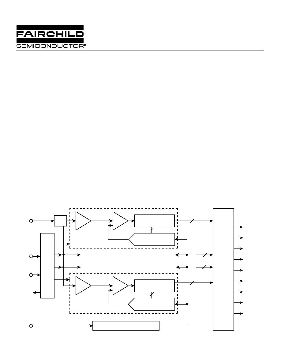
9-Bit
SAR
DAC
ADC Section 1
T/H
9
9-Bit
SAR
DAC
ADC Section 16
Auto-
Zero
CMP
Auto-
Zero
CMP
T/H
9
VREF
1:16
Mux
.
.
.
9
9
9
9
9-Bit
16:1
Mux/
Error
Correction
Timing
and
Control
P1
P2
P15
P16
ADC Section 2
ADC Section 15
.
.
.
Reference Ladder
Ref
In
Enable
CLK In
Data
Vali
d
A
IN
.
.
.
D8 Overrange
D7 (MSB)
D6
D5
D4
D3
D2
D1
DØ (LSB)
BLOCK DIAGRAM

2
1/27/98
SPT7734
ELECTRICAL SPECIFICATIONS
T
A
=T
MAX
to T
MAX
, AV
DD
=DV
DD
=+5.0 V, V
IN
=0 to 4 V, f
S
=40 MSPS, V
RHS
=4.0 V, V
RLS
=0.0 V, unless otherwise specified.
TEST
TEST
SPT7734
PARAMETERS
CONDITIONS
LEVEL
MIN
TYP
MAX
UNITS
Resolution
8
Bits
DC Accuracy
Integral Nonlinearity
IV
±
1.0
LSB
Differential Nonlinearity
IV
±
0.5
LSB
No Missing Codes
VI
Guaranteed
Analog Input
Input Voltage Range
VI
V
RLS
V
RHS
V
Input Resistance
IV
50
k
Input Capacitance
V
5.0
pF
Input Bandwidth
(Small Signal)
V
250
MHz
Offset
V
±
2.0
LSB
Gain Error
V
±
2.0
LSB
Reference Input
Resistance
VI
300
500
600
Bandwidth
V
100
150
MHz
Voltage Range
V
RLS
IV
0
-
2.0
V
V
RHS
IV
3.0
-
AV
DD
V
V
RHS
- V
RLS
V
1.0
4.0
5.0
V
(V
RHF
- V
RHS
)
V
90
mV
(V
RLS
- V
RLF
)
V
75
mV
Reference Settling Time
V
RHS
V
15
Clock Cycles
V
RLS
V
20
Clock Cycles
Conversion Characteristics
Maximum Conversion Rate
VI
40
MHz
Minimum Conversion Rate
IV
2
MHz
Pipeline Delay (Latency)
IV
12
Clock Cycles
Aperture Delay Time
V
4.0
ns
Aperture Jitter Time
V
30
ps(p-p)
Dynamic Performance
Effective Number of Bits
f
IN
=3.58 MHz
VI
7.3
7.8
Bits
f
IN
=10.3 MHz
VI
7.2
7.7
Bits
ABSOLUTE MAXIMUM RATINGS (Beyond which damage may occur)
1
25
°
C
Note:
1.
Operation at any Absolute Maximum Rating is not implied. See Electrical Specifications for proper nominal
applied conditions in typical applications.
Supply Voltages
AV
DD
......................................................................... +6 V
DV
DD
........................................................................ +6 V
Input Voltages
Analog Input .................................. -0.5 V to AV
DD
+0.5 V
V
REF ............................................................................
0 to AV
DD
CLK Input .................................................................. V
DD
AV
DD
- DV
DD ...............................................................
±
100 mV
AGND
- DGND ...................................................
±
100 mV
Output
Digital Outputs ....................................................... 10 mA
Temperature
Operating Temperature ................................. 0 to +70
°
C
Junction Temperature ......................................... +175
°
C
Lead Temperature, (soldering 10 seconds) ........ +300
°
C
Storage Temperature ................................ -65 to +150
°
C

3
1/27/98
SPT7734
ELECTRICAL SPECIFICATIONS
T
A
=T
MAX
to T
MAX
, AV
DD
=DV
DD
=+5.0 V, V
IN
=0 to 4 V, f
S
=40 MSPS, V
RHS
=4.0 V, V
RLS
=0.0 V, unless otherwise specified.
TEST
TEST
SPT7734
PARAMETERS
CONDITIONS
LEVEL
MIN
TYP
MAX
UNITS
Dynamic Performance
Signal-to-Noise Ratio
(without Harmonics)
f
IN
=3.58 MHz
VI
46
49
dB
f
IN
=10.3 MHz
VI
45
48
dB
Harmonic Distortion
9 Distortion bins from
f
IN
=3.58 MHz
1024 pt FFT
VI
53
57
dB
f
IN
=10.3 MHz
VI
53
56
dB
Signal-to-Noise and Distortion
(SINAD)
f
IN
=3.58 MHz
VI
46
49
dB
f
IN
=10.3 MHz
VI
45
48
dB
Spurious Free Dynamic Range
f
IN
=1.0 MHz
V
63
dB
Differential Phase
V
±
0.3
Degree
Differential Gain
V
±
0.3
%
Intermodulation Distortion
TBD
dB
Inputs
Logic 1 Voltage
VI
2.0
V
Logic 0 Voltage
VI
0.8
V
Maximum Input Current Low
VI
-10
+10
µ
A
Maximum Input Current High
VI
-10
+10
µ
A
Input Capacitance
V
+5
pF
Digital Outputs
Logic 1 Voltage
I
OH
= 0.5 mA
VI
3.5
V
Logic 0 Voltage
I
OL
= 1.6 mA
VI
0.4
V
t
RISE
15 pF load
V
10
ns
t
FALL
15 pF load
V
10
ns
Output Enable to Data Output Delay
20 pF load, T
A
= +25
°
C
V
10
ns
50 pF load over temp.
V
22
ns
Power Supply Requirements
Voltages
OV
DD
IV
3.0
5.0
V
DV
DD
IV
4.75
5.0
5.25
V
AV
DD
IV
4.75
5.0
5.25
V
Currents
AI
DD
VI
17
22
mA
DI
DD
VI
18
23
mA
Power Dissipation
VI
175
225
mW
TEST LEVEL CODES
All electrical characteristics are subject to the
following conditions:
All parameters having min/max specifications
are guaranteed. The Test Level column indi-
cates the specific device testing actually per-
formed during production and Quality Assur-
ance inspection. Any blank section in the data
column indicates that the specification is not
tested at the specified condition.
TEST PROCEDURE
100% production tested at the specified temperature.
100% production tested at T
A
=25
°
C, and sample
tested at the specified temperatures.
QA sample tested only at the specified temperatures.
Parameter is guaranteed (but not tested) by design
and characterization data.
Parameter is a typical value for information purposes
only.
100% production tested at T
A
= 25
°
C. Parameter is
guaranteed over specified temperature range.
TEST LEVEL
I
II
III
IV
V
VI
4
1/27/98
SPT7734
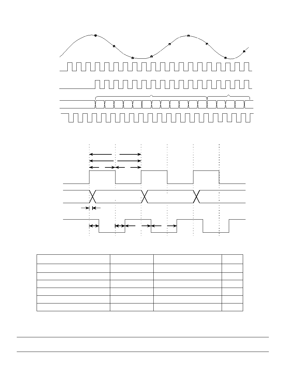
Figure 1A: Timing Diagram 1
DESCRIPTION
PARAMETERS
MIN
TYP
MAX
UNITS
Conversion Time
t
C
t
CLK
ns
Clock Period
t
CLK
25
ns
Clock High Duty Cycle
t
CH
40
50
60
%
Clock Low Duty Cycle
t
CL
40
50
60
%
Clock to Output Delay (15 pF Load)
t
OD
17
ns
Clock to DAV
t
S
10
ns
Table I - Timing Parameters
Figure 1B: Timing Diagram 2
ANALOG IN
CLOCK IN
1
3
5
7
9
11
13
15
17
SAMPLING
CLOCK
(Internal)
DATA OUTPUT
DATA VALID
VALID
INVALID
1
3
2
4
5
t
OD
t
CL
t
CH
t
C
t
CLK
Data Ø
Data 1
Data 2
Data 3
CLOCK IN
DATA
OUTPUT
DATA
VALID
t
S
t
CH
t
CL
t
S
5
1/27/98
SPT7734
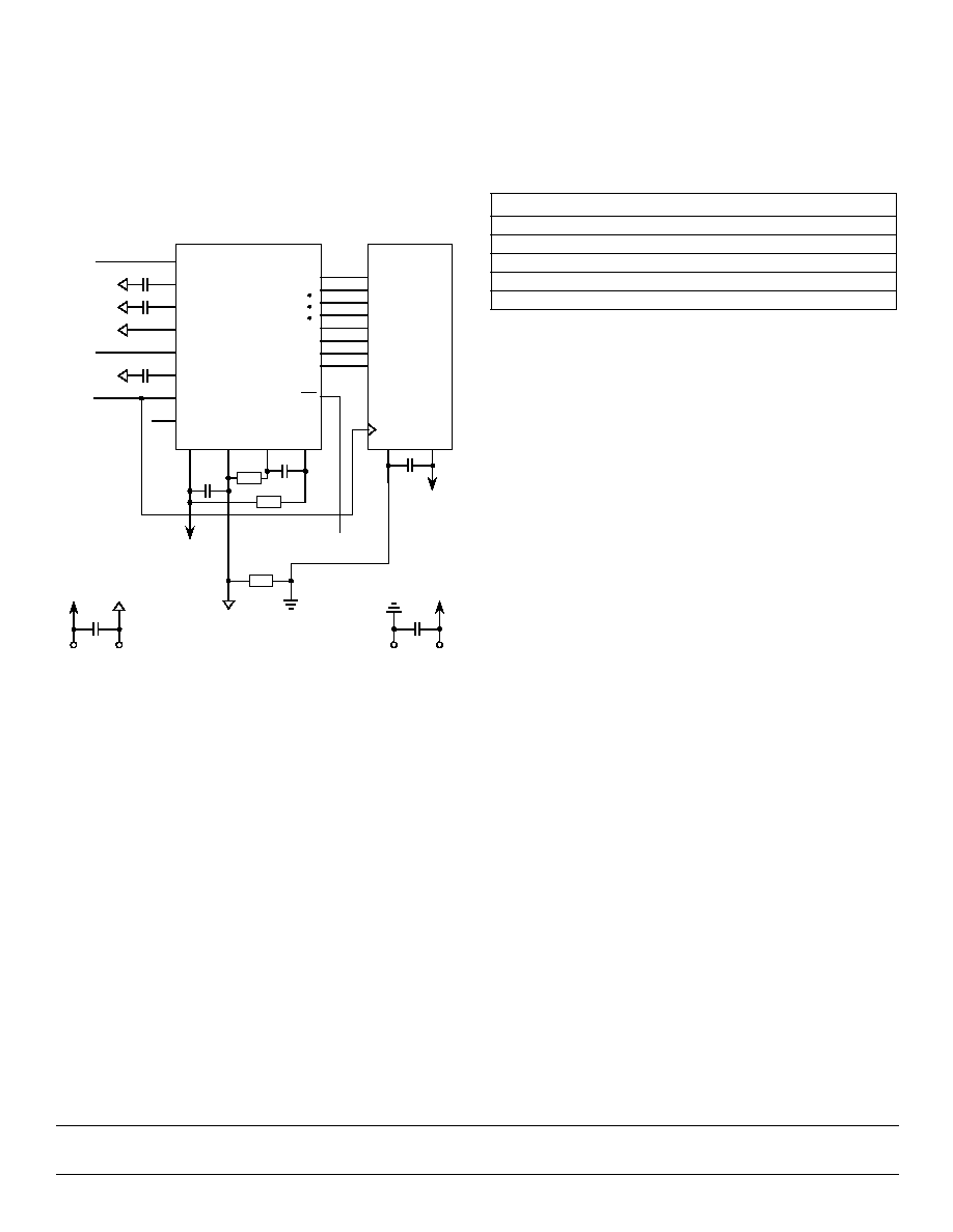
TYPICAL INTERFACE CIRCUIT
Very few external components are required to achieve the
stated device performance. Figure 1 shows the typical inter-
face requirements when using the SPT7734 in normal circuit
operation. The following sections provide descriptions of the
major functions and outline critical performance criteria to
consider for achieving the optimal device performance.
Figure 1 - Typical Interface Circuit
The high sample rate is achieved by using multiple SAR ADC
sections in parallel, each of which samples the input signal in
sequence. Each ADC uses 16 clock cycles to complete a
conversion. The clock cycles are allocated as follows:
Table II - Clock Cycles
Clock
Operation
1
Reference zero sampling
2
Auto-zero comparison
3
Auto-calibrate comparison
4
Input sample
5-15
9-bit SAR conversion
16
Data transfer
The 16 phase clock, which is derived from the input clock,
synchronizes these events. The timing signals for adjacent
ADC sections are shifted by one clock cycle so that the analog
input is sampled on every cycle of the input clock by exactly
one ADC section. After 16 clock periods, the timing cycle
repeats. The latency from analog input sample to the corre-
sponding digital output is 12 clock cycles.
· Since only 16 comparators are used, a huge power savings
is realized.
· The auto-zero operation is done using a closed loop
system that uses multiple samples of the comparators
response to a reference zero.
· The auto-calibrate operation, which calibrates the gain
of the MSB reference and the LSB reference, is also
done with a closed loop system. Multiple samples of the
gain error are integrated to produce a calibration voltage for
each ADC section.
· Capacitive displacement currents, which can induce sam-
pling error, are minimized since only one comparator
samples the input during a clock cycle.
· The total input capacitance is very low since sections of the
converter which are not sampling the signal are isolated
from the input by transmission gates.
VOLTAGE REFERENCE
The SPT7734 requires the use of a single external voltage
reference for driving the high side of the reference ladder. It
must be within the range of 3 V to 5 V. The lower side of the
ladder is typically tied to AGND (0.0 V), but can be run up to
2.0 V with a second reference. The analog input voltage
range will track the total voltage difference measured be-
tween the ladder sense lines, V
RHS
and V
RLS
.
Force and sense taps are provided to ensure accurate and
stable setting of the upper and lower ladder sense line
voltages across part-to-part and temperature variations. By
using the configuration shown in figure 2, offset and gain
errors of less than
±
2 LSB can be obtained.
POWER SUPPLIES AND GROUNDING
Fairchild suggests that both the digital and the analog supply
voltages on the SPT7734 be derived from a single analog
supply as shown in figure 1. A separate digital supply should
be used for all interface circuitry. Fairchild suggests using
this power supply configuration to prevent a possible latch-
up condition on power up.
OPERATING DESCRIPTION
The general architecture for the CMOS ADC is shown in the
block diagram. The design contains 16 identical successive
approximation ADC sections, all operating in parallel, a 16-
phase clock generator, an 9-bit 16:1 digital output multi-
plexer, correction logic, and a voltage reference generator
which provides common reference levels for each ADC section.
VRHF
VRLS
VRLF
VRHS
VIN
CLK
VCAL
DAV
D8
D0
EN
AVDD
AGND
DGND* DVDD
Ref In
(+4 V)
VIN
CLK IN
Enable/Tri-State
(Enable = Active Low)
Interfacing
Logics
+D5
SPT7734
DGND
+
10 µF
+5 V
Digital
+5 V
Digital
RTN
+D5
FB3
NOTES: 1) FB3 is to be located as closely to the device as possible.
2) There should be no additional connections to the right of FB1 and FB2.
3) All capacitors are 0.1 µF surface-mount unless otherwise specified.
4) FB1, FB2 and FB3 are 10 µH inductors or ferrite beads.
FB1
FB2
+A5
AGND
+
10 µF
+5 V
Analog
+5 V
Analog
RTN
+A5
*To reduce the possibility of latch-up, avoid
connecting the DGND pins of the ADC to the
digital ground of the system.