Äîêóìåíòàöèÿ è îïèñàíèÿ www.docs.chipfind.ru
SPT7750
8-BIT, 500 MSPS, FLASH A/D CONVERTER
TECHNICAL DATA
NOVEMBER 30, 2001
FEATURES
· 1:2 Demuxed ECL compatible outputs
· Wide input bandwidth 900 MHz
· Low input capacitance 15 pF
· Metastable errors reduced to 1 LSB
· Monolithic for low cost
· Gray code output
APPLICATIONS
· Digital oscilloscopes
· Transient capture
· Radar, EW, ECM
· Direct RF down-conversion
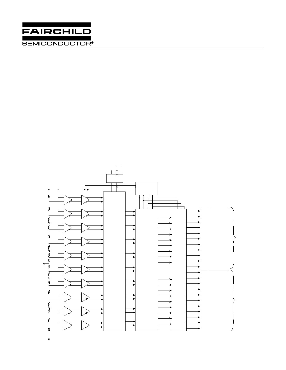
GENERAL DESCRIPTION
The SPT7750 is a full parallel (flash) analog-to-digital con-
verter capable of digitizing full scale (0 to 2 V) inputs into
eight-bit digital words at an update rate of 500 MSPS. The
ECL-compatible outputs are demultiplexed into two sepa-
rate output banks, each with differential data ready out-
puts to ease the task of data capture. The SPT7750's wide
input bandwidth and low capacitance eliminate the need
for external track-and-hold amplifiers for most applica-
tions. A proprietary decoding scheme reduces metastable
errors to the 1 LSB level. The SPT7750 operates from a
single 5.2 V supply, with a nominal power dissipation of
5.5 W.
The SPT7750 is available in an 80-lead surface-mount
MQuad package over the industrial temperature range
(25 °C to +85 °C) and in die form.
256
255
152
151
128
127
64
63
2
1
CLOCK
BUFFER
256 T
O 8 Bit Decoder
W
ith Metastable Error Correction
D0
(LSB)
D1
D2
D3
D4
D5
D6
D7
(MSB)
D8
(OVR)
V
RT
Analog
Input
Preamp
Comparator
V
RM
V
RB
CLK CLK
ECL Output Buffers And Latches
1:2 DEMUL
TIPLEXER
D8B
D7B
D6B
D5B
D4B
D3B
D2B
D1B
D0B
D8A
D7A
D6A
D5A
D4A
D3A
D2A
D1A
D0A
D8B (OVR)
D7B (MSB)
D6B
D5B
D4B
D3B
D2B
D1B
D0B (LSB)
D8A (OVR)
D7A (MSB)
D6A
D5A
D4A
D3A
D2A
D1A
D0A (LSB)
DRA (DATA READY)
DRA (DATA READY)
DEMUX
CLOCK
BUFFER
DRB (DATA READY)
DRB (DATA READY)
BANK A
BANK B
BLOCK DIAGRAM

2
11/30/01
SPT7750
ABSOLUTE MAXIMUM RATINGS (Beyond which damage may occur)
1
25 °C
Note: 1. Operation at any Absolute Maximum Rating is not implied. See
Electrical Specifications for proper nominal applied conditions
in typical applications.
ELECTRICAL SPECIFICATIONS
T
J
= T
C
= T
A
= +25 °C , V
EE
=5.2 V, V
RB
=2.0 V, V
RM
=1.0 V, V
RT
=0.00 V,
CLK
=500 MHz, Duty Cycle=50%, unless otherwise specified.
TEST
TEST
SPT7750A
SPT7750B
PARAMETERS
CONDITIONS
LEVEL
MIN
TYP
MAX
MIN
TYP
MAX UNITS
Resolution
8
8
Bits
DC Accuracy
Integral Linearity Error (ILE)
CLK
= 100 kHz
I
1.0
+1.0
1.5
+1.5
LSB
Differential Linearity Error
(DLE)
CLK
= 100 kHz
I
0.85
+0.95
0.95
+1.5
LSB
No Missing Codes
Guaranteed
Guaranteed
Analog Input
Input Voltage Range
I
V
RB
V
RT
V
RB
V
RT
V
Input Bias Current
V
IN
=0 V
I
.75
2.0
.75
2.0
mA
Input Resistance
V
15
15
k
Input Capacitance
Over Full Input Range
V
15
15
pF
Input Bandwidth
Small Signal
V
900
900
MHz
Large Signal
V
500
500
MHz
Offset Error V
RT
IV
30
+30
30
+30
mV
Offset Error V
RB
IV
30
+30
30
+30
mV
Input Slew Rate
V
5
5
V/ns
Clock Synchronous
Input Currents
V
2
2
µA
Reference Input
Ladder Resistance
I
60
80
60
80
Reference Bandwidth
V
30
30
MHz
Timing Characteristics
Maximum Sample Rate
I
500
500
MHz
Aperture Jitter
V
2
2
ps
Acquisition Time
V
250
250
ps
CLK to Data Ready Delay
IV
0.9
1.4
1.9
0.9
1.4
1.9
ns
Clock to Data Delay
IV
1.25
1.75
2.25
1.25
1.75
2.25
ns
Dynamic Performance
Signal-To-Noise Ratio
(without Harmonics)
IN
= 50 MHz
I
47
45
dB
IN
= 250 MHz
I
44
42
dB
Total Harmonic Distortion
IN
= 50 MHz
I
46
44
dBc
IN
= 250 MHz
I
38
36
dBc
Signal-to-Noise and Distortion
IN
= 50 MHz
I
43
41
dB
IN
= 250 MHz
I
37
35
dB
Supply Voltages
Negative Supply Voltage (V
EE
TO GND) 7.0 to +0.5 V
Ground Voltage Differential .................... 0.5 to +0.5 V
Input Voltage
Analog Input Voltage ............................... +0.5 V to V
EE
Reference Input Voltage .......................... +0.5 V to V
EE
Digital Input Voltage ................................ +0.5 V to V
EE
Reference Current V
RT
to V
RB
........................... 35 mA
Output
Digital Output Current ............................... 0 to 28 mA
Temperature
Operating Temperature, ambient ............ 25 to +85 °C
case .......................... +125 °C
junction ..................... +150 °C
Lead Temperature, (soldering 10 seconds) ..... +300 °C
Storage Temperature ............................ 65 to +150 °C

3
11/30/01
SPT7750
TEST LEVEL CODES
All electrical characteristics are subject to the
following conditions:
All parameters having min/max specifications
are guaranteed. The Test Level column indi-
cates the specific device testing actually per-
formed during production and Quality Assur-
ance inspection. Any blank section in the data
column indicates that the specification is not
tested at the specified condition.
Unless otherwise noted, all test are pulsed
tests; therefore, T
J
= T
C
= T
A
.
LEVEL
TEST PROCEDURE
I
100% production tested at the specified temperature.
II
100% production tested at T
A
= +25 °C, and sample tested at the
specified temperatures.
III
QA sample tested only at the specified temperatures.
IV
Parameter is guaranteed (but not tested) by design and characteri-
zation data.
V
Parameter is a typical value for information purposes only.
VI
100% production tested at T
A
= +25 °C. Parameter is guaranteed
over specified temperature range.
ELECTRICAL SPECIFICATIONS
T
J
= T
C
= T
A
= +25 °C , V
EE
=5.2 V, V
RB
=2.0 V, V
RM
=1.0 V, V
RT
=0.00 V,
CLK
=500 MHz, Duty Cycle=50%, unless otherwise specified.
TEST
TEST
SPT7750A
SPT7750B
PARAMETERS
CONDITIONS
LEVEL
MIN
TYP
MAX
MIN
TYP
MAX UNITS
Dynamic Performance
Spurious Free Dynamic Range
IN
= 50 MHz
I
49
44
dB
IN
= 250 MHz
I
41
36
dB
Digital Inputs
Input High Voltage
(CLK,
CLK
)
I
1.1
0.7
1.1
0.7
V
Input Low Voltage
(CLK,
CLK
)
I
1.8
1.5
1.8
1.5
V
Clock Pulse Width High (t
PWH
)
I
1.0
0.67
1.0
0.67
ns
Clock Pulse Width Low (t
PWL
)
I
1.0
0.67
1.0
0.67
ns
Digital Outputs
Logic 1 Voltage
I
1.1
0.9
1.1
0.9
V
Logic 0 Voltage
I
1.8
1.5
1.8
1.5
V
Rise Time
20% to 80%
V
450
450
ps
Fall Time
20% to 80%
V
450
450
ps
Power Supply Requirements
Voltage V
EE
IV
4.95
5.2
5.45
4.95
5.2
5.45 V
Current I
EE
I
1.05
1.2
1.05
1.2
A
Power Dissipation
I
5.5
6.25
5.5
6.25
W
Typical Thermal Impedance:
JC
= +4 °C/W.
4
11/30/01
SPT7750
GENERAL DESCRIPTION
The SPT7750 is one of the fastest monolithic 8-bit parallel
flash A/D converters available today. The nominal conver-
sion rate is 500 MSPS and the analog bandwidth is in
excess of 900 MHz. A major advance over previous flash
converters is the inclusion of 256 input preamplifiers
between the reference ladder and input comparators (see
block diagram). This not only reduces clock transient kick-
back to the input and reference ladder due to a low AC
beta, but also reduces the effect of the dynamic state of
the input signal on the latching characteristics of the input
comparators. The preamplifiers act as buffers and stabi-
lize the input capacitance so that it remains constant over
different input voltage and frequency ranges and therefore
makes the part easier to drive than previous flash convert-
ers. The preamplifiers also add a gain of two to the input
signal so that each comparator has a wider overdrive or
threshold range to "trip" into or out of the active state. This
gain reduces metastable states that can cause errors at
the output.
The SPT7750 has true differential analog and digital data
paths from the preamplifiers to the output buffers (Current
Mode Logic) for reducing potential missing codes while
rejecting common mode noise.
Signature errors are also reduced by careful layout of the
analog circuitry. The output drive capability of the device
can provide full ECL swings into 50
loads.
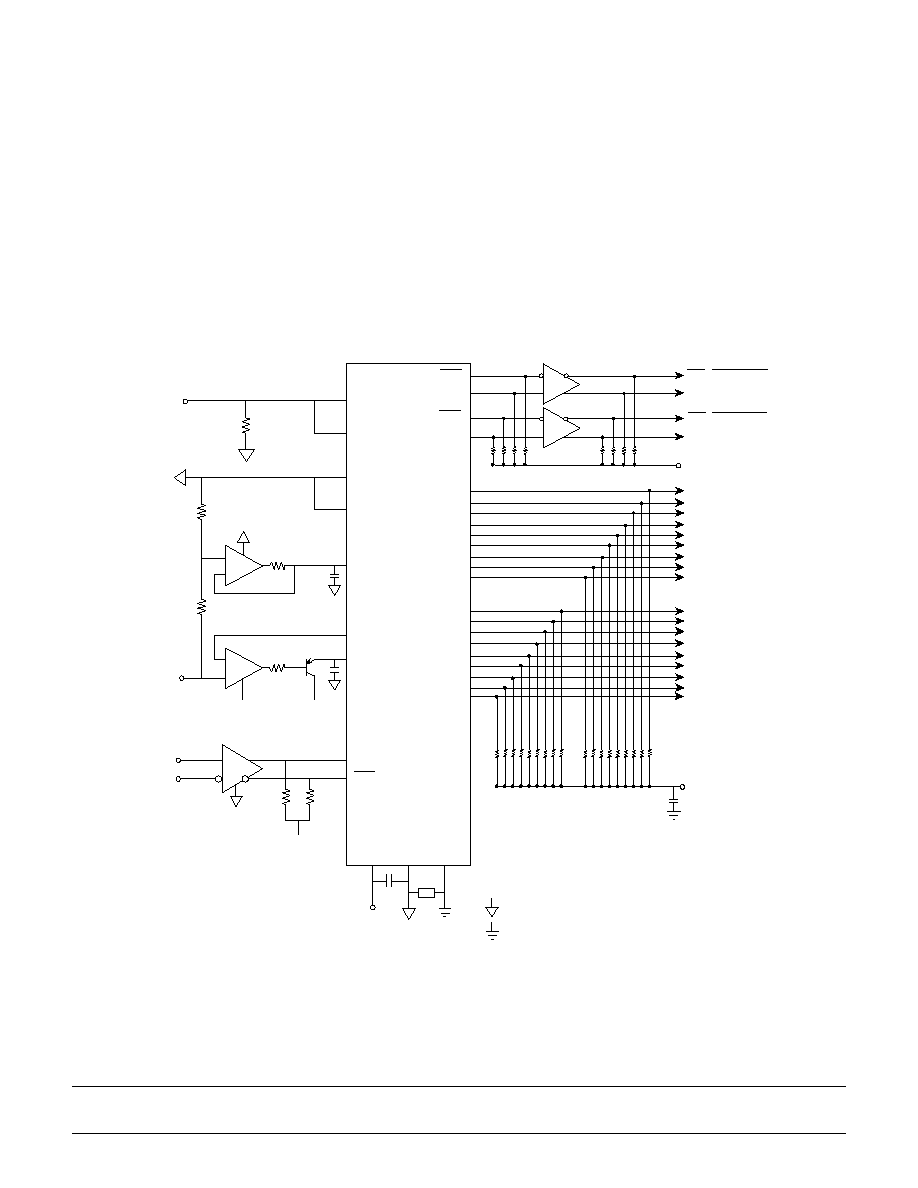
Figure 1 SPT7750 Typical Interface Circuit
50
W
50 W
V
IN
V
IN
V
RTF
V
RTS
*
U1
+
22 W
*
U1
+
22 W
5.2 V
2N2907
V
RBS
V
RBF
50 W
V
IN
**
2.0 V
Reference
Convert
U2
50 W
2 V
Pulldown
(Analog)
CLK
CLK
5.2 V
V
EE
AGND
DGND
V
RM
D8B (OVR)
D7B (MSB)
D6B
D5B
D4B
D3B
D2B
D1B
D0B (LSB)
D8A (OVR)
D7A (MSB)
D6A
D5A
D4A
D3A
D2A
D1A
D0A (LSB)
2.0 V
Pulldown
(Digital)
50
W
.1 µF
FB = Ferrite bead
U1 = OP291 or equivalent with low offset/noise.
R = 1 kW; 0.1% matched.
= AGND
= DGND
U2 = ON Semiconductor ECLinPS LITE, MC10EL16,
differential receiver with 250 ps (typ) propagation delay.
U3 = MC10EL16 or MC100EL16.
* = 10 µF Tantalum Capacitor and 0.1 µF Chip Capacitor
** = Care must be taken to avoid exceeding the maximum rating
for the input, especially during power up sequencing of the
analog input driver.
R
R
*
5.2 V
FB
DRB
DRB
DRA
DRA
U3
U3
DRA (DATA READY)
DRA (DATA READY)
DRB (DATA READY)
DRB (DATA READY)
50
W
2.0 V Pulldown (Digital)
50
W
5
11/30/01
SPT7750
TYPICAL INTERFACE CIRCUIT
The circuit in figure 1 is intended to show the most elabo-
rate method of achieving the least error by correcting for
integral linearity, input induced distortion, and power sup-
ply/ground noise. This is achieved by the use of external
reference ladder tap connections, input buffer, and supply
decoupling. Please contact the factory for the SPT7750
evaluation board application note that contains more
details on interfacing the SPT7750. The function of each
pin and external connections to other components is as
follows:
V
EE
, AGND, DGND
V
EE
is the supply pin with AGND as ground for the device.
The power supply pins should be bypassed as close to the
device as possible with at least a .01 µF ceramic capaci-
tor. A 10 µF tantalum can also be used for low frequency
suppression. DGND is the ground for the ECL outputs and
is to be referenced to the output pulldown voltage and ap-
propriately bypassed as shown in figure 1.
V
IN
(ANALOG INPUT)
There are two analog input pins that are tied to the same
point internally. Either one may be used as an analog input
sense and the other for input force. This is convenient for
testing the source signal to see if there is sufficient drive
capability. The pins can also be tied together and driven by
the same source. The SPT7750 is superior to similar de-
vices due to a preamplifier stage before the comparators.
This makes the device easier to drive because it has con-
stant capacitance and induces less slew rate distortion.
CLK,
CLK
(CLOCK INPUTS)
The clock inputs are designed to be driven differentially
with ECL levels. The duty cycle of the clock should be kept
at 50% to avoid causing larger second harmonics. If this is
not important to the intended application, then duty cycles
other than 50% may be used.
D0 TO D8, DR,
DR
, (A AND B)
The digital outputs can drive 50
to ECL levels when
pulled down to 2 V. When pulled down to 5.2 V, the out-
puts can drive 130
to 1 k
loads. All digital outputs are
grey code with the coding as shown in table I. Fairchild rec-
ommends using differential receivers on the outputs of the
data ready lines to ensure the proper output rise and fall
times.
V
RBF
, V
RBS
, V
RTF
, V
RTS
, V
RM
(REFERENCE INPUTS)
There are two reference inputs and one external reference
voltage tap. These are 2 V (V
RB
force and sense), mid-
tap (V
RM
) and AGND (V
RT
force and sense). The refer-
ence pins and tap can be driven by op amps as shown in
figure 1 or V
RM
may be bypassed for limited temperature
operation. These voltage inputs can be bypassed to
AGND for further noise suppression if so desired.
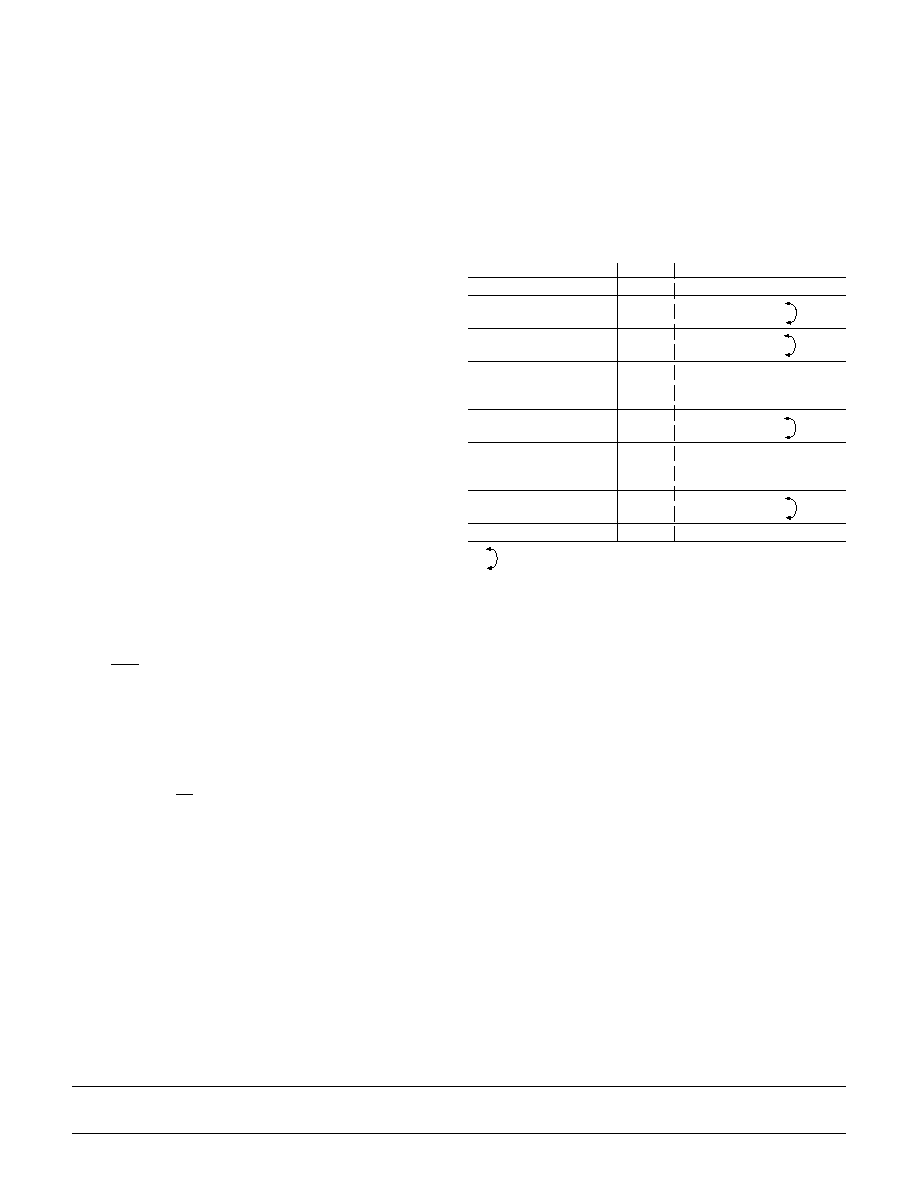
Table I Output Coding
V
IN
D8
D7 . . . D8
>0.5 LSB
1
1 0 0 0 0 0 0 0
0.5 LSB
1
1 0 0 0 0 0 0 0
0
1 0 0 0 0 0 0 0
1.5 LSB
0
1 0 0 0 0 0 0 0
0
1 0 0 0 0 0 0 1
·
·
·
·
·
·
·
·
·
1.0 V
0
1 1 0 0 0 0 0 0
0
0 1 0 0 0 0 0 0
·
·
·
·
·
·
·
·
·
2.0 V +0.5 LSB
0
0 0 0 0 0 0 0 1
0
0 0 0 0 0 0 0 0
<(2.0 V +0.5 LSB)
0
0 0 0 0 0 0 0 0
Indicates the transition between the two codes
THERMAL MANAGEMENT
The typical thermal impedance is as follows:
CA = +17 °C/W in still air with no heat sink
We highly recommend that a heat sink be used for this
device with adequate air flow to ensure rated performance
of the device. We have found that a Thermalloy 17846
heat sink with a minimum air flow of 1 meter/second (200
linear feet per minute) provides adequate thermal perfor-
mance under laboratory tests. Application specific condi-
tions should be taken into account to ensure that the
device is properly heat sinked.