Äîêóìåíòàöèÿ è îïèñàíèÿ www.docs.chipfind.ru
SPT7830
10-BIT, 2.5 MSPS, SERIAL OUTPUT A/D CONVERTER
10-Bit
A/D
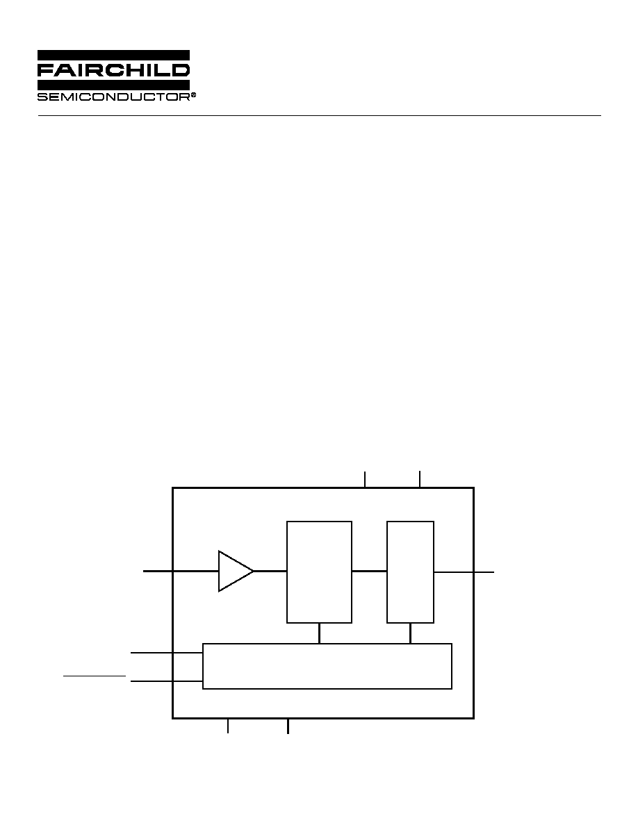
Analog Input
VREF+
Serial
Output
Logic
Ground
VDD
SAR
Clock
Data Out
Start Convert
Track-and-Hold
VREF-
Timing And Control
BLOCK DIAGRAM
FEATURES
· 10-Bit, 1 kHz to 2.5 MSPS Analog-to-Digital Converter
· Monolithic CMOS
· Serial Output
· Internal Sample-and-Hold
· Analog Input Range: 0 to 2 V Nominal; 3.3 V Max
· Power Dissipation (Excluding Reference Ladder)
45 mW at +5 V
16 mW at +3.0 V
· Single Power Supply: +3 V to +5 V Range
· High ESD Protection: 3,000 V Minimum
APPLICATIONS
· Handheld and Desktop Scanners
· DSP Interface Applications
· Portable Digital Radios
· Portable and Handheld Applications
· Automotive Applications
· Remote Sensing
GENERAL DESCRIPTION
The SPT7830 10-bit, 2.5 MSPS, serial analog-to-digital
converter delivers excellent high speed conversion perfor-
mance with low cost and low power. The serial port protocol
is compatible with the serial peripheral interface (SPI) or
MICROWIRETM
industry standard, high-speed synchronous
MPU interfaces. The large input bandwidth and fast transient
response time allow for CCD applications operating up to
2.5 MSPS.
The device can operate with a power supply range from
+3 V to +5 V with very low power dissipation. The small
package size makes this part excellent for hand-held appli-
cations where board space is at a premium. The SPT7830 is
available in an 8-lead SOIC package over the commercial
and industrial temperature ranges. Contact the factory for
availability of die.

2
12/29/99
SPT7830
ELECTRICAL SPECIFICATIONS
T
A
= +25
°
C, V
DD
= +5.0 V, V
IN
= 0 to +3 V, f
CLK
= 35 MHz, f
S
= 2.5 MSPS, V
REF
+ = +3.0 V, V
REF
= 0.0 V, unless otherwise specified.
TEST
TEST
PARAMETERS
CONDITIONS
LEVEL
MIN
TYP
MAX
UNITS
DC ELECTRICAL CHARACTERISTICS
DC Performance
Resolution
10
Bits
Differential Linearity
VI
±
0.5
±
1.0
LSB
Integral Linearity
VI
±
1.0
±
1.5
LSB
No Missing Codes
VI
Guaranteed
Analog Input
Input Voltage Range
1
IV
V
REF
+4%
V
REF
+
6%
V
Input Resistance
VI
5
M
Input Capacitance
IV
5
pF
Input Bandwidth (Small Signal)
IV
30
MHz
Offset
IV
2
+2
% of FSR
Gain Error
IV
2
+2
% of FSR
Reference Input
Resistance
IV
250
280
350
Voltage Range
1
V
REF
2
IV
4%
0
V
REF
+
V
V
REF
+
2
IV
V
REF
+
2/3 V
DD
V
V
REF
+
V
REF
(
)
IV
1/10 V
DD
V
Reference Settling Time
IV
90
ns
Timing Characteristics
Maximum Conversion Rate
VI
2.5
1.0
MSPS
Minimum Conversion Rate
IV
1
kSPS
Maximum External Clock Rate
VI
35
14
MHz
Minimum External Clock Rate
IV
14
kHz
Aperture Delay Time
IV
5
ns
Aperture Jitter Time
IV
5
ps
Data Output LSB Hold Time
T
MIN
to T
MAX
IV
6
8
ns
Supply Voltages
V
DD
...........................................................................+6 V
Input Voltages
Analog Input ................................................ 0.7 to +6 V
V
REF
+ .......................................................... 0.7 to +6 V
V
REF
.......................................................... 0.7 to +6 V
Clock and
SC
.............................................. 0.7 to +6 V
Output
Data Out ................................................................ 10 mA
Temperature
Operating,
ambient ............................... 40 to +85
°
C
junction ......................................... +175
°
C
Lead, Soldering (10 seconds) ............................ +300
°
C
Storage .................................................... 65 to +150
°
C
Note: 1. Operation at any Absolute Maximum Ratings is not implied. See Electrical Specifications for proper nominal applied
conditions in typical applications.
1
Percentages refer to percent of [(V
REF
+) (V
REF
)]
2
= Minimum (V
REF
+
V
REF
)
ABSOLUTE MAXIMUM RATING (Beyond which damage may occur)
1

3
12/29/99
SPT7830
ELECTRICAL SPECIFICATIONS
T
A
= +25
°
C, V
DD
= +5.0 V, V
IN
= 0 to +3 V, f
CLK
= 35 MHz, f
S
= 2.5 MSPS, V
REF
+ = +3.0 V, V
REF
= 0.0 V, unless otherwise specified.
TEST
TEST
PARAMETERS
CONDITIONS
LEVEL
MIN
TYP
MAX
UNITS
Dynamic Performance
Effective Number of Bits
f
IN
= 500 kHz
IV
8.9
Bits
f
IN
= 1 MHz
IV
8.5
Bits
Signal-to-Noise Ratio
f
IN
= 500 kHz
IV
56
dB
f
IN
= 1 MHz
IV
55
dB
Harmonic Distortion
f
IN
= 500 kHz
IV
63
dB
f
IN
= 1 MHz
IV
58
dB
Power Supply Requirements
+V
DD
Supply Voltage
IV
3
5.5
V
+V
DD
Supply Current
V
DD
= +3.0 V
IV
5.4
7
mA
V
DD
= +5.0 V
VI
9
10
mA
Power Dissipation
3
V
DD
= +3.0 V
IV
16
22
mW
V
DD
= +5.0 V
VI
45
50
mW
3
Excluding reference ladder.
TEST LEVEL CODES
All electrical characteristics are subject to the
following conditions:
All parameters having min/max specifications
are guaranteed. The Test Level column indi-
cates the specific device testing actually per-
formed during production and Quality Assur-
ance inspection. Any blank section in the data
column indicates that the specification is not
tested at the specified condition.
TEST PROCEDURE
100% production tested at the specified temperature.
100% production tested at T
A
=+25
°
C, and sample
tested at the specified temperatures.
QA sample tested only at the specified temperatures.
Parameter is guaranteed (but not tested) by design
and characterization data.
Parameter is a typical value for information purposes
only.
100% production tested at T
A
= +25
°
C. Parameter is
guaranteed over specified temperature range.
TEST LEVEL
I
II
III
IV
V
VI

4
12/29/99
SPT7830
should be taken to ensure that the LSB is latched into an
external latch with the proper amount of set and hold time.
DATA OUTPUT CODING
The coding of the output is straight binary. (See table I.)
Table I - Data Output Coding
ANALOG INPUT
OUTPUT CODE D9 - DO
+FS -1/2 LSB
1 1
1 1 1 1
1 1 1 Ø
+1/2 FS
ØX
X X X X
X X X X
+1/2 LSB
OO
OOOO
OOOØ
V
REF-
OO
OOOO
OOOO
Ø indicates the flickering bit between logic O and 1.
X indicates the flickering bit between logic 1 and O.
ANALOG INPUT AND REFERENCE SETTLING TRACK
AND HOLD TIMING
Figure 9 shows the timing relationship between the input
clock and
SC
versus the analog input tracking and reference
settling. The analog input is tracked from the fourteenth clock
cycle of the previous conversion to the third clock cycle of the
current conversion. On the falling edge of the third clock
cycle, the analog input is held by the internal sample-and-
hold. After this sample, the analog input may vary without
affecting data conversion.
The reference ladder inputs (V
REF
+ and V
REF
-) may be
changed starting on the falling edge of the thirteenth clock
cycle of the previous conversion and must be settled by the
falling edge of the third clock cycle of the current conversion.
VOLTAGE REFERENCE AND ANALOG INPUT
The SPT7830 requires the use of a single external voltage
reference for driving the high side of the reference ladder.
The V
REF
+ can be a maximum of 2/3 V
DD
. For example, if
V
DD
= +5 V, then V
REF
+ max = (2/3) * 5 V = +3.3 V. The lower
side of the ladder is typically tied to AGND (0.0 V), but can be
run up to a voltage that is 1/10th of V
DD
below V
REF
+:
V
REF
- max. = V
REF
+ - (1/10) * V
DD
.
For example,
if V
DD
= +5 V and V
REF
+ = 3 V, then
V
REF
- max = 3 V - (1/10)* 5 V = 2.5 V.
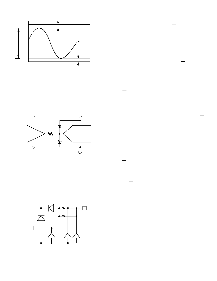
The +Full Scale (+FS) of the analog input is expected to be 6%
of [(V
REF
+) - (V
REF
-)] below V
REF
+ and the -Full Scale (-FS)
of the analog input is expected to be 4% of [(V
REF
+) - (V
REF
-)]
above V
REF
-. (See figure 1.)
Therefore,
Analog +FS = V
REF
+ - 0.06 * [(V
REF
+) - (V
REF
-)], and
Analog -FS = V
REF
- +0.04 * [(V
REF
+) - (V
REF
-)].
For example,
if V
REF
+ = 3 V and V
REF
- = 0 V, then
Analog +FS = 3 V - 0.06 * [3 V- 0 V ] = 2.82 V, and
Analog -FS = 0 V + 0.04 * [3 V - 0 V] = 0.12 V.
GENERAL DESCRIPTION AND OPERATION
The SPT7830 is a 10-bit analog-to-digital converter that
uses a successive approximation architecture to perform
data conversion. Each conversion cycle is 14 clocks in
length. When the Not Start Convert (
SC
) line is held low,
conversion begins on the next rising edge of the input clock.
When the conversion cycle begins, the data output pin is
forced low until valid data output begins.
The first two clock cycles are used to perform internal offset
calibrations and tracking of the analog input. The analog input
is then sampled using an internal track-and-hold amplifier on
the falling edge of the third clock cycle. On clock cycles 4
through 14, a 10-bit successive approximation conversion is
performed, and the data is output starting with the MSB.
Serial data output begins with output of the MSB. See the
Data Output Timing section for details. Each bit of the data
conversion is sequentially determined and placed on the
data output pin at the clock rate. This process continues until
the LSB has been determined and output. At this point, if the
SC
line is high, the data output pin will be forced into a high
impedance state, and the converter will go into an idle state
waiting for the
SC
line to go low. This is referred to as Single
Shot Mode. See Modes of Operation for details.
If the
SC
is either held low through the entire 14 clock
conversion cycle (free run mode) or is brought low prior to
the trailing edge of the fourteenth clock cycle (synchronous
mode), the data output pin goes low and stays low until valid
data output begins. Because the chip has either remained
selected in the free run mode or has been immediately
selected again in the synchronous mode, the next conversion
cycle begins immediately after the fourteenth clock cycle of
the previous conversion. See Modes of Operation for details.
TYPICAL INTERFACE CIRCUIT
CLOCK INPUT
The SPT7830 requires a 50%
±
10% duty cycle clock running
at 14 times the desired sample rate. The clock may be
stopped in between conversion cycles without degradation
of operation (single shot type of operation); however, the
clock should remain running during a conversion cycle.
POWER SUPPLY
The SPT7830 requires only a single supply and operates
from 3.0 V to 5.0 V. Fairchild recommends that a 0.01
µ
F chip
capacitor be placed as close as possible to the supply pin.
DATA OUTPUT SET UP AND HOLD TIMING
As figure 8 shows, all of the data output bits (except the LSB)
remain valid for a duration equivalent to one clock period and
delayed by 8 ns after the falling edge of clock. Because the
data converter enters into a next conversion ready state at
the leading edge of clock 14, the LSB bit is valid for a
duration equivalent to only the clock pulse width low
and delayed by 8 ns after the falling edge of clock. Care
5
12/29/99
SPT7830
Figure 1 - Analog Input Full-Scale Range
V
REF
+
6% of [(V
REF
+) - (V
REF
-)]
V
REF
-
+FS
-FS
Full-Scale Range
4% of [(V
REF
+) - (V
REF
-)]
The drive requirements for the analog input are minimal
when compared to most other converters due to the
SPT7830's extremely low input capacitance of only 5 pF and
very high input resistance of greater than 5 M
.
If the input buffer amplifier supply voltages are greater than
V
DD
+ 0.7 V or less than Ground - 0.7 V, the analog input
should be protected through a series resistor and a diode
clamping circuit as shown in figure 2.
Figure 2 - Recommended Input Protection Circuit
47
D1
D2
ADC
Buffer
AV
DD
+V
-V
D1 = D2 = Hewlett Packard HP5712 or equivalent
INPUT PROTECTION
All I/O pads are protected with an on-chip protection circuit
shown in figure 3. This circuit provides ESD robustness to
>3.0 kV and prevents latch-up under severe discharge
conditions without degrading analog transition times.
Figure 3 - On-Chip Protection Circuit
V
DD
Analog
Pad
120
120
MODES OF OPERATION
The SPT7830 has three modes of operation.The mode of
operation is based strictly on how the
SC
is used.
SINGLE SHOT MODE
When
SC
goes low, conversion starts on the next rising edge
of the clock (defined as the first conversion clock). The MSB
of data is valid 8 ns after the falling edge of the fourth
conversion clock. (See figure 8, Data Output Timing.)
The conversion is complete after 14 clock cycles. At the
falling edge of the fourteenth clock cycle, if
SC
is high (not
selected), the data output goes to a high impedance state,
and no more conversions will take place until the next
SC
low
event. (See the single shot mode timing diagram in figure 4.)
SYNCHRONIZED MODE
When
SC
goes low, conversion will start on the next rising
edge of the clock (defined as the first conversion clock). The
MSB is valid 8 ns after the falling edge of the fourth conver-
sion clock.
The first conversion is complete after 14 clock cycles. At any
time after the falling edge of the fourteenth clock cycle,
SC
may go low again to initiate the next conversion. When the
SC
goes low, the conversion starts on the rising edge of the
next clock. (See the synchronized mode timing diagram in
figure 5.)
The data output will go to a high impedance state until the
next conversion is initiated.
FREE RUN MODE
When
SC
goes low, conversion starts on the next rising edge
of the clock (defined as the first conversion clock). The MSB
data is valid 8 ns after the falling edge of the fourth conver-
sion clock.
As long as
SC
is held low, the device operates in the free run
mode. New conversions start after every fourteenth cycle
with valid data available 8 ns after the falling edge of the
fourth clock within each new conversion cycle.
The data output remains low between conversion cycles.
(See the free run mode timing diagram in figure 6.)