 | –≠–ª–µ–∫—Ç—Ä–æ–Ω–Ω—ã–π –∫–æ–º–ø–æ–Ω–µ–Ω—Ç: SPT7835 | –°–∫–∞—á–∞—Ç—å:  PDF PDF  ZIP ZIP |

SPT7835
10-BIT, 5 MSPS, 75 mW A/D CONVERTER
TECHNICAL DATA
JUNE 27, 2001
FEATURES
∑ Monolithic 5 MSPS converter
∑ 75 mW power dissipation
∑ On-chip track-and-hold
∑ Single +5 V power supply
∑ TTL/CMOS outputs
∑ 5 pF input capacitance
∑ Low cost
∑ Tri-state output buffers
∑ High ESD protection: 3,500 V minimum
∑ Selectable +3 V or +5 V logic I/O
APPLICATIONS
∑ All high-speed applications where low power
dissipation is required
∑ Video imaging
∑ Medical imaging
∑ IR imaging
∑ Scanners
∑ Digital communications
GENERAL DESCRIPTION
The SPT7835 is a 10-bit monolithic, low-cost, ultralow-
power analog-to-digital converter capable of minimum
word rates of 5 MSPS. The on-chip track-and-hold func-
tion assures very good dynamic performance without the
need for external components. The input drive require-
ments are minimized due to the SPT7835's low input
capacitance of only 5 pF.
Power dissipation is extremely low at only 75 mW typical
at 5 MSPS with a power supply of +5.0 V. The digital out-
puts are +3 V or +5 V, and are user selectable. The
SPT7835 is pin-compatible with an entire family of 10-bit,
CMOS converters (SPT7835/40/50/55/60/61), which sim-
plifies upgrades. The SPT7835 has incorporated propri-
etary circuit design* and CMOS processing technologies
to achieve its advanced performance. Inputs and outputs
are TTL/CMOS-compatible to interface with TTL/CMOS
logic systems. Output data format is straight binary.
The SPT7835 is available in a 28-lead SOIC package over
the industrial temperature range, and a 32-lead small
(7 mm square) TQFP package over the commercial
temperature range.
*Patent pending
BLOCK DIAGRAM
11-Bit
SAR
DAC
ADC Section 1
T/H
11
11-Bit
SAR
DAC
ADC Section 8
Auto-
Zero
CMP
Auto-
Zero
CMP
T/H
11
V
REF
1:8
Mux
11
11
11
11
11-Bit
8:1
Mux/
Error
Correction
Timing
and
Control
P1
P2
P7
P8
ADC Section 2
ADC Section 7
Reference Ladder
Ref
In
Enable
CLK In
Data
Valid
A
IN
D10 Overrange
D9 (MSB)
D8
D7
D6
D5
D4
D3
D2
D1
D0 (LSB)
.
.
.
.
.
.
.
.
.
.
.
.

2
6/27/01
SPT7835
ABSOLUTE MAXIMUM RATINGS (Beyond which damage may occur)
1
25 ∞C
Note: 1. Operation at any Absolute Maximum Rating is not implied. See
Electrical Specifications for proper nominal applied conditions
in typical applications.
ELECTRICAL SPECIFICATIONS
T
A
=T
MIN
to T
MAX
, AV
DD
=DV
DD
=OV
DD
=+5.0 V, V
IN
=0 to 4 V,
CLK
=10 MHz,
S
=5 MSPS, V
RHS
=4.0 V, V
RLS
=0.0 V, unless otherwise specified.
TEST
TEST
SPT7835
PARAMETERS
CONDITIONS
LEVEL
MIN
TYP
MAX
UNITS
Resolution
10
Bits
DC Accuracy
Integral Linearity Error (ILE)
VI
±1.0
LSB
Differential Linearity Error (DLE)
VI
±0.5
LSB
No Missing Codes
VI
Guaranteed
Analog Input
Input Voltage Range
VI
V
RLS
V
RHS
V
Input Resistance
IV
50
k
Input Capacitance
V
5.0
pF
Input Bandwidth
(Small Signal)
V
100
MHz
Offset
V
±2.0
LSB
Gain Error
V
±2.0
LSB
Reference Input
Resistance
VI
400
500
600
Bandwidth
V
100
150
MHz
Voltage Range
V
RLS
IV
0
2.0
V
V
RHS
IV
3.0
AV
DD
V
V
RHS
≠ V
RLS
V
1.0
4.0
5.0
V
(V
RHF
≠ V
RHS
)
V
90
mV
(V
RLS
≠ V
RLF
)
V
75
mV
Reference Settling Time
V
RHS
V
15
Clock Cycles
V
RLS
V
20
Clock Cycles
Conversion Characteristics
Maximum Conversion Rate
VI
5
MHz
Minimum Conversion Rate
IV
2
MHz
Pipeline Delay (Latency)
IV
12
Clock Cycles
Aperture Delay Time
V
5
ns
Aperture Jitter Time
V
10
ps (p-p)
Dynamic Performance
Effective Number of Bits (ENOB)
IN
= 1 MHz
VI
9.2
Bits
Signal-to-Noise Ratio (SNR)
(without Harmonics)
IN
= 1 MHz
VI
54
59
dB
Supply Voltages
AV
DD
...................................................................... +6 V
DV
DD
..................................................................... +6 V
Input Voltages
Analog Input .............................. ≠0.5 V to AV
DD
+0.5 V
V
REF
.............................................................. 0 to AV
DD
CLK Input ............................................................... V
DD
AV
DD
≠ DV
DD
.................................................. ±100 mV
AGND ≠ DGND .............................................. ±100 mV
Output
Digital Outputs ................................................... 10 mA
Temperature
Operating Temperature ............................ ≠40 to 85 ∞C
Junction Temperature ........................................ 175 ∞C
Lead Temperature, (soldering 10 seconds) ....... 300 ∞C
Storage Temperature ............................ ≠65 to +150 ∞C

3
6/27/01
SPT7835
TEST LEVEL CODES
All electrical characteristics are subject to the
following conditions:
All parameters having min/max specifications
are guaranteed. The Test Level column indi-
cates the specific device testing actually per-
formed during production and Quality Assur-
ance inspection. Any blank section in the data
column indicates that the specification is not
tested at the specified condition.
LEVEL
TEST PROCEDURE
I
100% production tested at the specified temperature.
II
100% production tested at T
A
= +25 ∞C, and sample tested at the
specified temperatures.
III
QA sample tested only at the specified temperatures.
IV
Parameter is guaranteed (but not tested) by design and characteri-
zation data.
V
Parameter is a typical value for information purposes only.
VI
100% production tested at T
A
= +25 ∞C. Parameter is guaranteed
over specified temperature range.
ELECTRICAL SPECIFICATIONS
T
A
=T
MIN
to T
MAX
, AV
DD
=DV
DD
=OV
DD
=+5.0 V, V
IN
=0 to 4 V,
CLK
=10 MHz,
S
=5 MSPS, V
RHS
=4.0 V, V
RLS
=0.0 V, unless otherwise specified.
TEST
TEST
SPT7835
PARAMETERS
CONDITIONS
LEVEL
MIN
TYP
MAX
UNITS
Dynamic Performance
Total Harmonic Distortion (THD)
IN
= 1 MHz
VI
59
63
dB
Signal-to-Noise and Distortion
(SINAD)
IN
= 1 MHz
VI
52
57
dB
Spurious Free Dynamic Range
V
63
dB
Digital Inputs
Logic 1 Voltage
VI
2.0
V
Logic 0 Voltage
VI
0.8
V
Maximum Input Current Low
VI
≠10
+10
µA
Maximum Input Current High
VI
≠10
+10
µA
Input Capacitance
V
5
pF
Digital Outputs
Logic 1 Voltage
I
OH
= 0.5 mA
VI
3.5
V
Logic 0 Voltage
I
OL
= 1.6 mA
VI
0.4
V
t
RISE
15 pF load
V
10
ns
t
FALL
15 pF load
V
10
ns
Output Enable to Data Output Delay 20 pF load, T
A
= +25 ∞C
V
10
ns
50 pF load over temp.
V
22
ns
Power Supply Requirements
Voltages
OV
DD
IV
3.0
5.0
V
DV
DD
IV
4.75
5.0
5.25
V
AV
DD
IV
4.75
5.0
5.25
V
Currents
AI
DD
VI
9
12
mA
DI
DD
VI
6
10
mA
Power Dissipation
IN
= 1 MHz
VI
75
110
mW

4
6/27/01
SPT7835
APERTURE DELAY
Aperture delay represents the point in time, relative to the
rising edge of the CLOCK input, that the analog input is
sampled.
APERTURE JITTER
The variations in aperture delay for successive samples.
DIFFERENTIAL GAIN (DG)
A signal consisting of a sine wave superimposed on vari-
ous DC levels is applied to the input. Differential gain is the
maximum variation in the sampled sine wave amplitudes
at these DC levels.
DIFFERENTIAL PHASE (DP)
A signal consisting of a sine wave superimposed on vari-
ous DC levels is applied to the input. Differential phase is
the maximum variation in the sampled sine wave phases
at these DC levels.
EFFECTIVE NUMBER OF BITS (ENOB)
SINAD = 6.02N + 1.76, where N is equal to the effective
number of bits.
INTEGRAL LINEARITY ERROR (ILE)
Linearity error refers to the deviation of each individual
code (normalized) from a straight line drawn from ≠FS
through +FS. The deviation is measured from the edge of
each particular code to the true straight line.
OUTPUT DELAY
Time between the clock's triggering edge and output data
valid.
OVERVOLTAGE RECOVERY TIME
The time required for the ADC to recover to full accuracy
after an analog input signal 125% of full scale is reduced
to 50% of the full-scale value.
SIGNAL-TO-NOISE RATIO (SNR)
The ratio of the fundamental sinusoid power to the total
noise power. Harmonics are excluded.
SIGNAL-TO-NOISE AND DISTORTION (SINAD)
The ratio of the fundamental sinusoid power to the total
noise and distortion power.
TOTAL HARMONIC DISTORTION (THD)
The ratio of the total power of the first 9 harmonics to the
power of the measured sinusoidal signal.
SPURIOUS FREE DYNAMIC RANGE (SFDR)
The ratio of the fundamental sinusoidal amplitude to the
single largest harmonic or spurious signal.
INPUT BANDWIDTH
Small signal (50 mV) bandwidth (3 dB) of analog input
stage.
DIFFERENTIAL LINEARITY ERROR (DLE)
Error in the width of each code from its theoretical value.
(Theoretical = V
FS
/2
N
)
N =
SINAD ≠ 1.76
6.02
SPECIFICATION DEFINITIONS
5
6/27/01
SPT7835
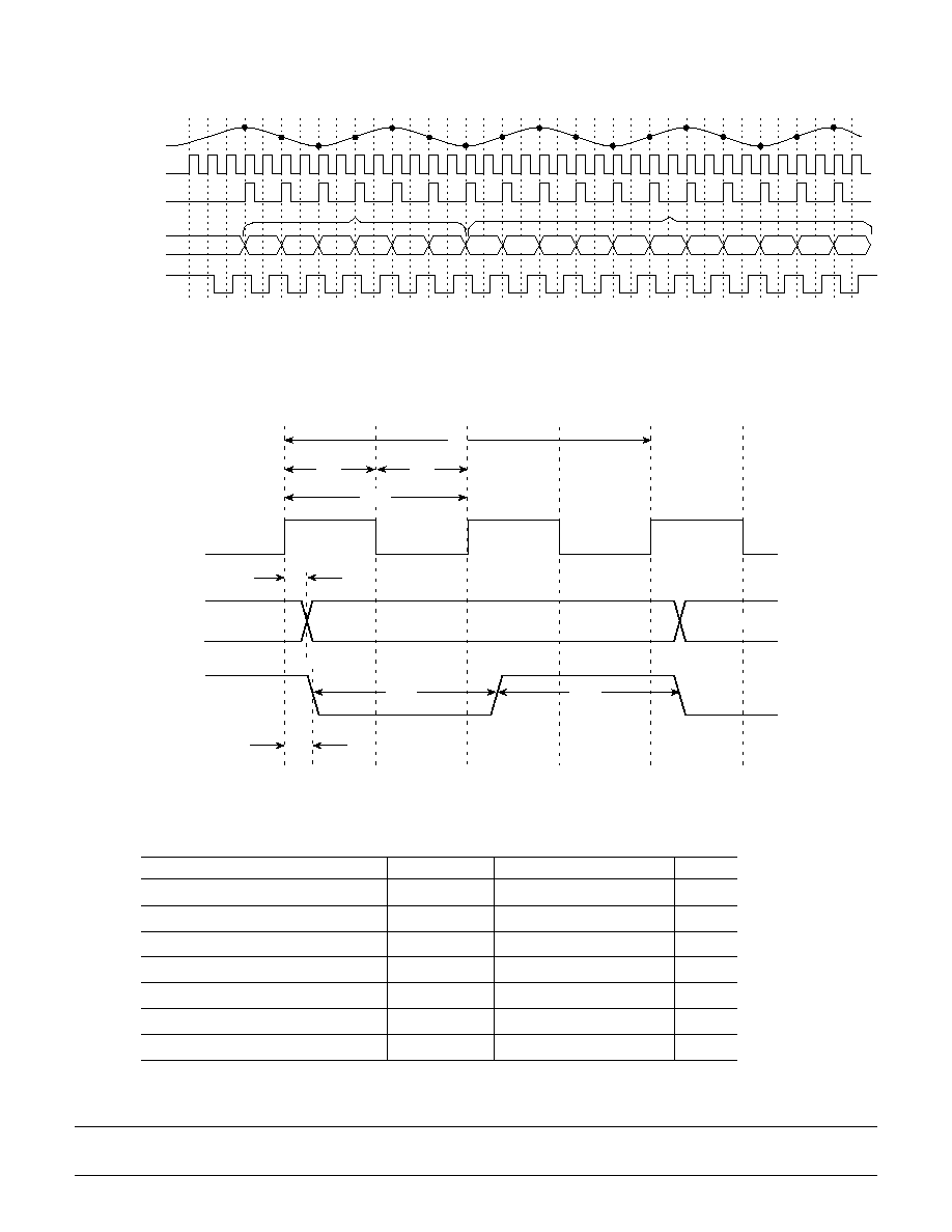
Figure 1A ≠ Timing Diagram 1
Figure 1B ≠ Timing Diagram 2
Table I ≠ Timing Parameters
DESCRIPTION
PARAMETERS
MIN
TYP
MAX
UNITS
Conversion Time
t
C
2*t
CLK
ns
Clock Period
t
CLK
100
ns
Clock High Duty Cycle
t
CH
40
50
60
%
Clock Low Duty Cycle
t
CL
40
50
60
%
Clock to Output Delay (15 pF Load)
t
OD
15
20
25
ns
DAV Pulse Width
t
DAV
t
CLK
ns
Clock to DAV
t
S
16
21
26
ns
4
ANALOG IN
CLOCK IN
SAMPLING CLOCK
(Internal)
DIGITAL OUT
DATA VALID
1
2
3
4
5
6
7
8
9
10
11
12
13
14
15
16
17
VALID
INVALID
5
6
7
1
2
3
8
9
10
11
DATA
VALID
DATA
OUTPUT
CLOCK
IN
Data 0
Data 1
Data 2
t
C
t
CL
t
CH
t
CLK
t
OD
t
DAV
t
DAV
t
S