SPT7852
DUAL 10-BIT, 20 MSPS, 160 mW A/D CONVERTER
FEATURES
∑ Dual 10-Bit/20 MSPS Analog-to-Digital Converter
∑ Monolithic CMOS
∑ Internal Track-and-Hold
∑ Low Power Dissipation: 160 mW
∑ 4 Vp-p Analog Input Range for Each ADC
∑ Single +5 Volt Power Supply
with Option for 3.3 V Digital Outputs
∑ Tri-State, TTL-Compatible Outputs
∑ Overrange Bit
∑ Selectable Two's Complement or Straight Binary Output
APPLICATIONS
∑ Video Set-Top Boxes
∑ Cellular Base Stations
∑ QPSK/QAM RF Demodulation
∑ S-Video Digitizers
∑ Composite Video Digitizers
∑ Portable and Handheld Instrumentation
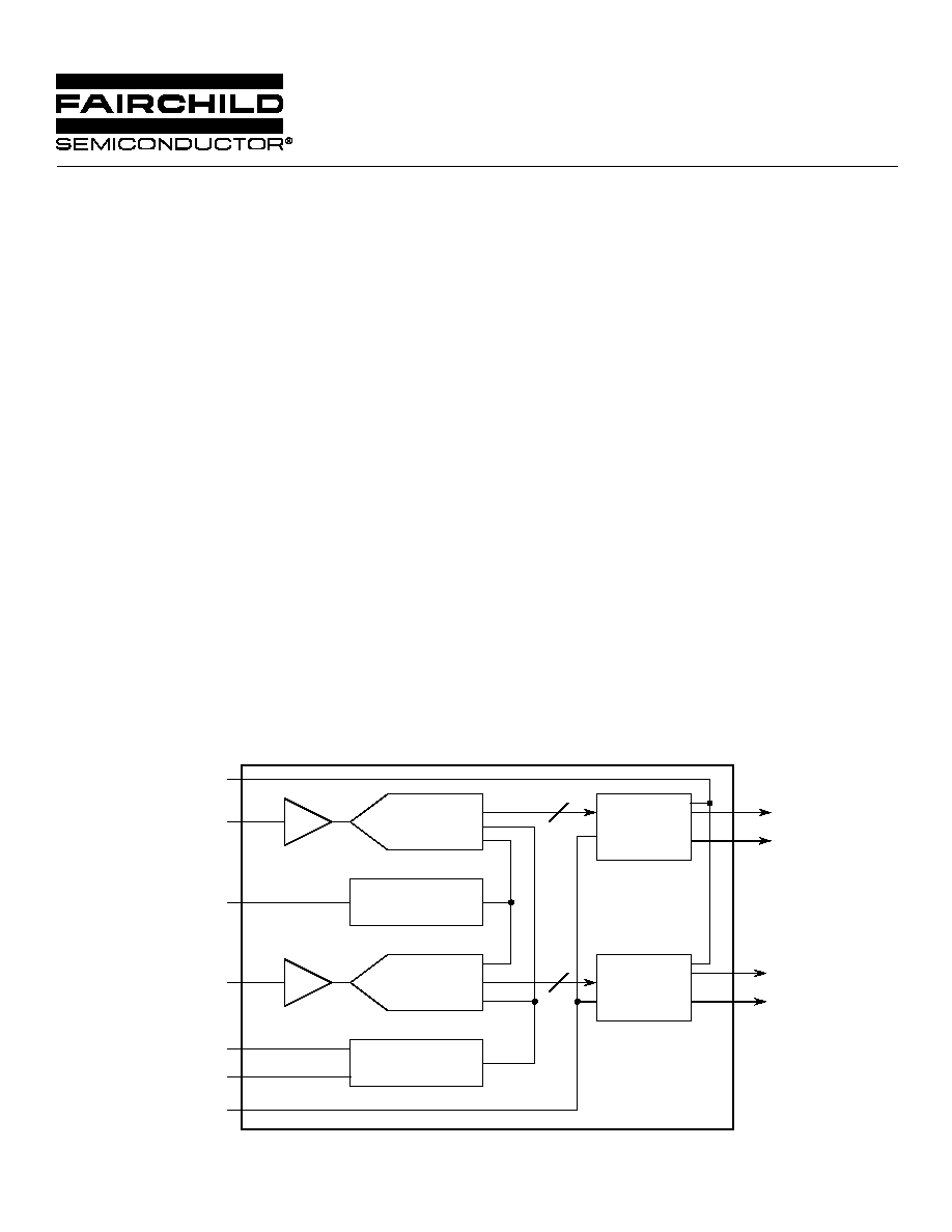
Overrange
DA0-9
Overrange
DB0-9
ADCA
Reference
Ladder
ADCB
Timing
Generation
Output
Buffer
Output
Buffer
10
10
VINB
MSB
Invert
Clock
Output
Enable
VINA
Reference In
Reset
T/H
T/H
BLOCK DIAGRAM
GENERAL DESCRIPTION
The SPT7852 has two 10-Bit CMOS analog-to-digital con-
verters that can sample data at speeds up to 20 MSPS. It
has excellent low noise performance with a very low typical
power dissipation of only 160 mW--that's the total power
for
both converters. The SPT7852 uses a dual configuration
of the proprietary circuit design found in our 10-bit CMOS
single converter family, to achieve its high performance in a
CMOS process.
The SPT7852 is specifically designed for video decoding
applications and is ideal for S-video decoding and decoding
of multiple composite video sources. It also has excellent
application in the area of coherent I/Q demodulation in such
applications as QAM demodulation and TV set-top box con-
verters.
Inputs and outputs are TTL/CMOS-compatible to interface
with TTL/CMOS-logic systems. Output data format is select-
able for either straight binary or two's complement. The
SPT7852 is available in a 44L TQFP package in commercial
and industrial temperature ranges. It is also available in die
form. For availability of extended temperature ranges,
please contact the factory.

2
1/12/00
SPT7852
ELECTRICAL SPECIFICATIONS FOR EACH CHANNEL
T
A
= T
MIN
to T
MAX
, AV
DD
= DV
DD
= +5.0 V, V
IN
=0 to 4 V,
S
=20 MSPS,
CLK
=40 MHz, V
RHS
=4.0 V, V
RLS
=0.0 V, unless otherwise specified.
TEST
TEST
PARAMETERS
CONDITIONS
LEVEL
MIN
TYP
MAX
UNITS
Resolution
10
Bits
DC Accuracy
Integral Nonlinearity
IV
±
1.0
LSB
Differential Nonlinearity
IV
±
1.0
LSB
Analog Input
Input Voltage Range
V
V
RLS
V
RHS
V
Input Resistance
V
50
k
Input Capacitance
V
5.0
pF
Input Bandwidth
Full Power
V
35
MHz
Offset
VI
±
2.0
LSB
Gain Error
VI
±
2.0
LSB
Reference Input
Resistance
V
RHS
≠ V
RLS
VI
350
425
500
Voltage Range
V
RLS
IV
0
-
2.0
V
V
RHS
IV
3.0
-
AV
DD
V
V
RHS
≠ V
RLS
V
1.0
4.0
5.0
V
(V
RHF
≠ V
RHS
)
V
150
mV
(V
RLS
≠ V
RLF
)
V
150
mV
Conversion Characteristics
Maximum Conversion Rate
1
VI
20
MHz
Minimum Conversion Rate
1
IV
100
kHz
Pipeline Delay (Latency)
IV
12
Clock Cycles
Aperture Delay Time
V
5
ns
Aperture Jitter Time
V
15
ps
Dynamic Performance
Effective Number of Bits
IN
=3.58 MHz
VI
8.4
8.9
Bits
IN
= 10 MHz
VI
7.9
8.4
Bits
1
2X Clock required.
ABSOLUTE MAXIMUM RATINGS (Beyond which damage may occur)
1
25
∞
C
Supply Voltages
AV
DD
......................................................................... +6 V
DV
DD
......................................................................... +6 V
Input Voltages
Analog Input ................................. ≠0.5 V to AV
DD
+0.5 V
V
Ref
.............................................. ≠1.5 V to AV
DD
+0.8 V
CLK Input ................................................................... V
DD
AV
DD
≠ DV
DD
......................................................
±
100 mV
Output
Digital Outputs ....................................................... 10 mA
Temperature
Operating Temperature ................................... 0 to 70
∞
C
Junction Temperature ........................................... 175
∞
C
Lead Temperature, (soldering 10 seconds) .......... 300
∞
C
Storage Temperature ............................... ≠65 to +150
∞
C
Note:
1.
Operation at any Absolute Maximum Rating is not implied. See Electrical Specifications for proper nominal
applied conditions in typical applications.

3
1/12/00
SPT7852
ELECTRICAL SPECIFICATIONS
T
A
=T
MIN
to T
MAX
, AV
DD
= DV
DD
= +5.0 V, V
IN
=0 to 4 V,
S
=20 MSPS,
CLK
=40 MHz, V
RHS
= 4.0 V, V
RLS
=0.0 V, unless otherwise specified.
TEST
TEST
PARAMETERS
CONDITIONS
LEVEL
MIN
TYP
MAX
UNITS
Dynamic Performance
Signal-to-Noise Ratio
(without Harmonics)
IN
=3.58 MHz
VI
53
57
dB
IN
=10 MHz
VI
52
56
dB
Harmonic Distortion
IN
=3.58 MHz
VI
56
59
dB
IN
=10 MHz
VI
52
54
dB
Signal-to-Noise and Distortion
(SINAD)
IN
=3.58 MHz
VI
52
55
dB
IN
=10 MHz
VI
49
52
dB
Channel-to-Channel Crosstalk
IN
=3.58 MHz
IV
70
dB
Channel-to-Channel Gain Matching Full Scale
IV
0.04
dB
Spurious Free Dynamic Range
IN
=3.58 MHz @ ≠3 dB FS
V
66
dB
Differential Phase
V
0.2
Degree
Differential Gain
V
0.3
%
Digital Inputs
Logic "1" Voltage
VI
2.0
V
Logic "0" Voltage
VI
0.8
V
Maximum Input Current Low
V
IL
=0 V
VI
≠10
+10
µ
A
Maximum Input Current High
V
IH
=5 V
VI
≠10
+10
µ
A
Input Capacitance
V
5
pF
Digital Outputs
Logic "1" Voltage
I
OH
=0.5 mA
VI
OV
DD
≠0.5
V
Logic "0" Voltage
I
OS
=1.6 mA
VI
0.4
V
t
RISE
/t
FALL
15 pF Load
V
10
ns
Output Enable to Data Output Delay
20 pF Load, T
A
=+25
∞
C
V
10
ns
50 pF Load Over Temp.
V
22
ns
Power Supply Requirements
Voltages DV
DD
IV
4.75
5.0
5.25
V
AV
DD
IV
4.75
5.0
5.25
V
OV
DD
IV
2.7
5.0
5.25
V
Currents AI
DD
Total for Both Converter
VI
15
18
mA
DI
DD
Channels
VI
17
20
mA
Power Dissipation
VI
160
190
mW
TEST LEVEL CODES
All electrical characteristics are subject to the follow-
ing conditions:
All parameters having min/max specifications are
guaranteed. The Test Level column indicates the
specific device testing actually performed during
production and Quality Assurance inspection. Any
blank section in the data column indicates that the
specification is not tested at the specified condition.
TEST PROCEDURE
100% production tested at the specified temperature.
100% production tested at T
A
=+25
∞
C, and sample tested at
the specified temperatures.
QA sample tested only at the specified temperatures.
Parameter is guaranteed (but not tested) by design and char-
acterization data.
Parameter is a typical value for information purposes only.
100% production tested at T
A
= +25
∞
C. Parameter is guaran-
teed over specified temperature range.
TEST LEVEL
I
II
III
IV
V
VI
4
1/12/00
SPT7852
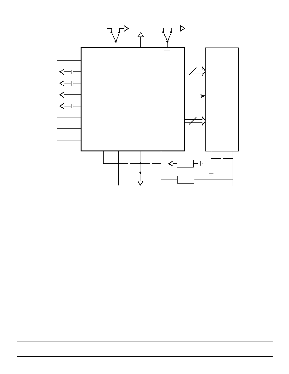
1. Place the ferrite bead (*) as close to the ADC as possible.
2. Place 0.1
µ
F decoupling capacitors as close to the ADC as possible.
3. All capacitors are 0.1
µ
F surface-mount unless otherwise specified.
4. All analog input pins (references, analog input, clock input) must
be protected. (See absolute maximum ratings.)
11
V
RHF
V
RHS
V
IN1
V
IN2
Clock
Ref In
(+4 V)
V
RLS
V
RLF
V
CAL
V
INA
V
INB
CLK
.1
µ
F
.1
µ
F
4.7
µ
F
4.7
µ
F
+A5
Interfacing
Logic
11
3.3 V/5 V
FB
*
+A5
MSBINV
Reset
Digital
Output A
Digital
Output B
DAV
SPT7852
AV
DD
DV
DD
GND
OV
DD
+A5
EN
EN
3-st
FB
*
Figure 1 ≠Typical Interface Circuit
TYPICAL INTERFACE CIRCUIT
Very few external components are required to achieve the
stated device performance. Figure 1 shows the typical inter-
face requirements when using the SPT7852 in normal
circuit operation. The following sections provide descrip-
tions of the major functions and outline critical performance
criteria to consider for achieving the optimal device perfor-
mance.
POWER SUPPLIES AND GROUNDING
Fairchild suggests that both the digital and the analog sup-
ply voltages on the SPT7852 be derived from a single ana-
log supply as shown in figure 1. A separate digital supply
must be used for all interface circuitry. Fairchild suggests
using this power supply configuration to prevent a possible
latch-up condition on powerup.

5
1/12/00
SPT7852
OPERATING DESCRIPTION
The general architecture for the CMOS ADC is shown in the
block diagram. The design contains two sets of eight identical
successive approximation ADC sections, all operating in par-
allel, a 16-phase clock generator, an 11-bit 8:1 digital output
multiplexer, correction logic, and a voltage reference genera-
tor which provides common reference levels for each ADC
section.
The high sample rate is achieved by using multiple SAR
ADC sections in parallel, each of which samples the input
signal in sequence. Each ADC uses 16 clock cycles to
complete a conversion. The clock cycles are allocated as
follows:
Table I ≠ Clock Cycles
Clock
Operation
1
Reference zero sampling
2
Auto-zero comparison
3
Auto-calibrate comparison
4
Input sample
5≠15
11-bit SAR conversion
16
Data transfer
The 16-phase clock, which is derived from the input clock,
synchronizes these events. The timing signals for adjacent
ADC sections are shifted by two clock cycles so that the
analog input is sampled on every other cycle of the input
clock by exactly one ADC section. After 16 clock periods,
the timing cycle repeats. The sample rate for the configura-
tion is one-half of the clock rate, e.g., for a 40 MHz clock
rate, the input sample rate is 20 MHz. The latency from ana-
log input sample to the corresponding digital output is 12
clock cycles.
∑ Since only sixteen comparators are used, a huge power
savings is realized.
∑ The auto-zero operation is done using a closed loop sys-
tem that uses multiple samples of the comparator's re-
sponse to a reference zero.
∑ The auto-calibrate operation, which calibrates the gain of
the MSB reference and the LSB reference, is also done
with a closed loop system. Multiple samples of the gain
error are integrated to produce a calibration voltage for
each ADC section.
∑ Capacitive displacement currents, which can induce sam-
pling error, are minimized since only one comparator per
V
IN
input samples the input during a clock cycle.
∑ The total input capacitance is very low since sections of
the converter which are not sampling the signal are iso-
lated from the input by transmission gates.