 | ÐлекÑÑоннÑй компоненÑ: SPT7853 | СкаÑаÑÑ:  PDF PDF  ZIP ZIP |
Äîêóìåíòàöèÿ è îïèñàíèÿ www.docs.chipfind.ru
SPT7853
TRIPLE 10-BIT, 30 MSPS A/D CONVERTER
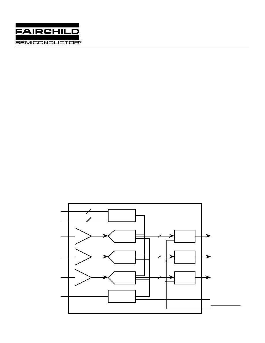
BLOCK DIAGRAM
GENERAL DESCRIPTION
The SPT7853 has three 10-bit analog-to-digital converters
on one CMOS chip, each with a sample rate of 30 MSPS.
This device is ideal for professional-level video decoding to
4:2:2/4:4:4 CCIR-601 standard specifications for compo-
nent digital video, including YCrCb and RGB decoding, pro-
fessional video equipment, video frame grabbers, medical
imaging, flat panel display and projection applications.
The SPT7853 offers significant advantages over discrete
single-channel A/D implementations. Board area, package
count, system cost and power dissipation can greatly be
reduced by using a single SPT7853 device. In addition,
several performance advantages exist, including low chan-
nel-to-channel cross-talk noise and well matched channel-
to-channel gain specifications. The three analog-to-digital
converters are driven from a common 2X sample rate
CMOS clock.
The SPT7853 typically consumes only 580 mW of total
power from a single +5 V supply. Digital outputs can operate
with +3 V or +5 V logic and are tri-state capable. The
SPT7853 is offered in a small 52-pin thin quad flat pack
(TQFP) package and operates over the 0 to +70
°
C com-
mercial temperature range.
APPLICATIONS
· CCIR-601 (4:2:2/4:4:4) digital component video
· RGB video decoding
· Medical imaging
· Flat panel displays
· PC projectors
FEATURES
· Three 10-bit, 30 MSPS ADCs on one chip
· SINAD of 54.5 dB @
IN
= 3.58 MHz
· Channel-to-channel cross talk: 66 dB typical
· Channel-to-channel gain matching of <0.1 dB
· Single 2X sample rate clock
· Total power dissipation: 580 mW (typical)
· Tri-state +3 V to +5 V digital outputs CMOS-compatible
· Single +5 V power supply
Timing
Generation
Reference
Ladder
ADC
A
ADC
B
ADC
C
T/H
T/H
T/H
10
10
10
V
IN
B
DA09
Clock
V
IN
A
V
IN
C
DB09
DC09
V
RH
Force/Sense
2
V
RL
Force/Sense
2
Output Enable
Output
Buffer
Output
Buffer
Output
Buffer
DAV

2
12/14/99
SPT7853
ELECTRICAL SPECIFICATIONS
T
A
=T
MIN
to T
MAX
, V
DD
=OV
DD
=+5.0 V, V
IN
=0 to 4 V,
S
=30 MSPS,
CLK
=60 MHz, V
RHS
=4.0 V, V
RLS
=0.0 V, unless otherwise specified.
TEST
TEST
SPT7853
PARAMETERS
CONDITIONS
LEVEL
MIN
TYP
MAX
UNITS
DC Performance
Resolution
10
Bits
Differential Linearity
s = 20 MSPS
V
±
0.5
LSB
Integral Linearity
s = 20 MSPS
V
±
1.0
LSB
Analog Input
Input Voltage Range
2
IV
V
RLS
V
RHS
V
Input Resistance
IV
50
k
Input Capacitance
V
5
pF
Input Bandwidth (Full Power)
V
120
MHz
Full-Scale Error
2
V
±
0.5
%FS
+Full-Scale Error
2
V
±
0.25
%FS
Reference Ladder Resistance
VI
120
170
220
Timing Characteristics
Conversion Rate
VI
30
MSPS
Clock Duty Cycle Range
IV
45
55
%
Clock-to-Sample Rate Relationship
IV
2:1
Pipeline Delay (Latency)
IV
12
Clock Cycles
Aperture Delay Time
V
5
ns
Aperture Jitter Time
V
15
ps
Dynamic Performance
Effective Number of Bits
IN
= 3.58 MHz
@ 25
°
C
VI
8.3
8.7
Bits
@ 0 to 70
°
C
V
8.0
Bits
IN
= 10.0 MHz
@ 25
°
C
V
7.4
Bits
Signal-to-Noise Ratio
IN
= 3.58 MHz
@ 25
°
C
VI
53
56
dB
@ 0 to 70
°
C
V
51.6
dB
IN
= 10.0 MHz
@ 25
°
C
V
48
dB
Total Harmonic Distortion
IN
= 3.58 MHz
@ 25
°
C
VI
56
58
dB
@ 0 to 70
°
C
V
54.6
dB
IN
= 10.0 MHz
@ 25
°
C
V
51
dB
Signal-to-Noise + Distortion Ratio
IN
= 3.58 MHz
@ 25
°
C
VI
52
54.5
dB
@ 0 to 70
°
C
V
49.7
dB
IN
= 10.0 MHz
@ 25
°
C
V
46
dB
Supply Voltages
V
DD ....................................................................................................
+6 V
OV
DD .................................................................................................
+6 V
Temperature
Analog Inputs .................................. 0.5 V to V
DD
+0.5 V
V
REF
................................................ 0.5 V to V
DD
+0.5 V
Clock Input ...................................... 0.5 V to V
DD
+0.5 V
Output Currents
Digital Outputs ....................................................... 10 mA
Temperature
Operating Temperature ................................ 0 to + 70
°
C
Junction Temperature ......................................... +150
°
C
Lead, Soldering (10 seconds) ............................. +300
°
C
Storage .................................................... 65 to +150
°
C
Note:
1. Operation at any Absolute Maximum Rating is not implied and operation beyond the ratings may cause damage to the device.
See Electrical Specifications for proper nominal applied conditions in typical applications.
ABSOLUTE MAXIMUM RATINGS (Beyond which damage may occur)
1
25
°
C
2
The full-scale range spans the reference ladder sense pins, V
RHS
and V
RLS
. Refer to the Voltage Reference section for discussion.

3
12/14/99
SPT7853
ELECTRICAL SPECIFICATIONS
T
A
=T
MIN
to T
MAX
, V
DD
=OV
DD
=+5.0 V, V
IN
=0 to 4 V,
S
=30 MSPS,
CLK
=60 MHz, V
RHS
=4.0 V, V
RLS
=0.0 V, unless otherwise specified.
TEST
TEST
SPT7853
PARAMETERS
CONDITIONS
LEVEL
MIN
TYP
MAX
UNITS
Dynamic Performance
Spurious Free Dynamic Range
IN
= 3.58 MHz
@ 25
°
C
V
65
dBc
@ 0 to 70
°
C
V
56.3
dBc
Channel-to-Channel Cross Talk
IN
= 3.58 MHz
V
66
dB
Channel-to-Channel Gain Matching
V
±
0.1
dB
Differential Phase
V
0.5
Degree
Differential Gain
V
0.5
%
Power Supply Requirements
V
DD
Supply Voltage
IV
+4.75
+5.0
+5.25
V
OV
DD
Supply Voltage
IV
+2.7
+5.25
V
Supply Current
I
DD
VI
81
105
mA
OI
DD
V
9
11
mA
Power Dissipation
Without reference ladder
C
L
= 10 pF
V
485
mW
Including reference ladder
C
L
= 10 pF
VI
580
750
mW
Digital Inputs/Outputs
Digital Input Logic 1 Voltage
VI
4.0
V
Digital Input Logic 0 Voltage
VI
1.0
V
Digital Output Logic 1 Voltage
I
OH
= 500
µ
A
VI
OV
DD
0.5
V
Digital Output Logic 0 Voltage
I
OL
= 800
µ
A
VI
0.4
V
t
RISE
/t
FALL
(C
L
= 10 pF)
V
10
ns
OEN to Data Output
V
12
ns
TEST LEVEL CODES
All electrical characteristics are subject to the
following conditions:
All parameters having min/max specifications
are guaranteed. The Test Level column indi-
cates the specific device testing actually per-
formed during production and Quality Assur-
ance inspection. Any blank section in the data
column indicates that the specification is not
tested at the specified condition.
TEST PROCEDURE
100% production tested at the specified temperature.
100% production tested at T
A
= +25
°
C, and sample
tested at the specified temperatures.
QA sample tested only at the specified temperatures.
Parameter is guaranteed (but not tested) by design and
characterization data.
Parameter is a typical value for information purposes
only.
100% production tested at T
A
= +25
°
C. Parameter is
guaranteed over specified temperature range.
TEST LEVEL
I
II
III
IV
V
VI
4
12/14/99
SPT7853
4
ANALOG IN
CLOCK IN
SAMPLING CLOCK
DIGITAL OUT
DATA VALID
1
2
3
4
5
6
7
8
9
10
11
12
13
14
15
16
17
(Internal)
VALID
INVALID
5
6
7
1
2
3
8
9
10
11
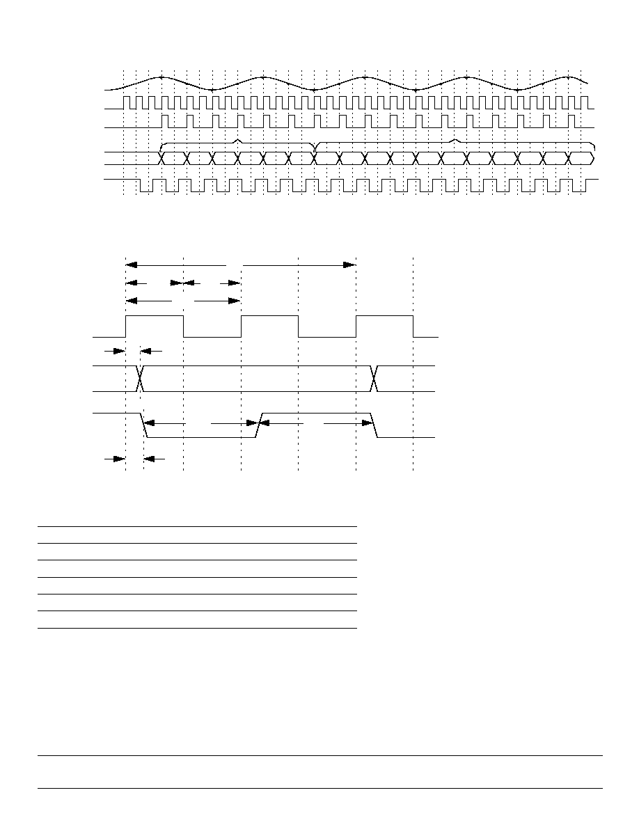
Figure 1a Timing Diagram 1
Figure 1b Timing Diagram 2
Table I Timing Parameters
Description
Parameters
Min
Typ
Max
Units
Conversion time
t
C
2 x t
CLK
nS
Clock period
t
CLK
16.67
nS
Clock duty cycle
45
50
55
%
Clock to output delay (15 pF load)
t
OD
19
nS
DAV pulse width
t
DAV
t
CLK
nS
Clock to DAV
t
D
6.5
nS
DATA
VALID
DATA
OUTPUT
DA, DB, DC
CLOCK
IN
t
OD
t
S
Data 0
Data 1
Data 2
t
C
t
CH
t
CL
t
CLK
t
DAV
t
DAV
5
12/14/99
SPT7853
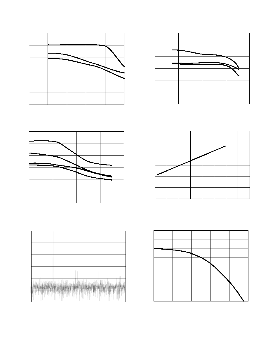
TYPICAL PERFORMANCE CHARACTERISTICS
65
60
55
50
45
40
35
0
2
6
8
10
THD
SNR
SINAD
THD, SNR, SINAD vs Input Frequency
Input Frequency (MHz)
THD
, SNR, SINAD (dB)
4
80
70
60
50
40
30
20
0
10
20
30
40
THD
SNR
SINAD
THD, SNR, SINAD vs Sample Rate
Sample Rate (MSPS)
THD
, SNR, SINAD (dB)
IN
=3.58 MHz
70
65
60
55
50
45
40
0
20
40
60
80
THD
SNR
SINAD
THD, SNR, SFDR, SINAD vs Temperature
Temperature (
°
C)
THD
, SNR, SFDR, SINAD (dB)
SFDR
600
500
400
300
200
100
0
0
5
10
15
20
Power Dissipation vs Sample Rate
1
Sample Rate (MSPS)
P
o
w
er Dissipation (mW)
25
30
35
40
Note 1: Power dissipation does not include reference.
0
0.5
1.0
1.5
2.0
2.5
3.0
0
25
50
75
100
125
Large Signal Bandwidth
Frequency (MHz)
dB
0.5
1.0
0
20
40
60
80
100
120
0
5
10
15
x106
Spectral Response
Frequency (MHz)
Amplitude (dB)
CLK 30 MHz
IN
=3.58 MHz