SPT7871
10-BIT, 100 MSPS TTL A/D CONVERTER
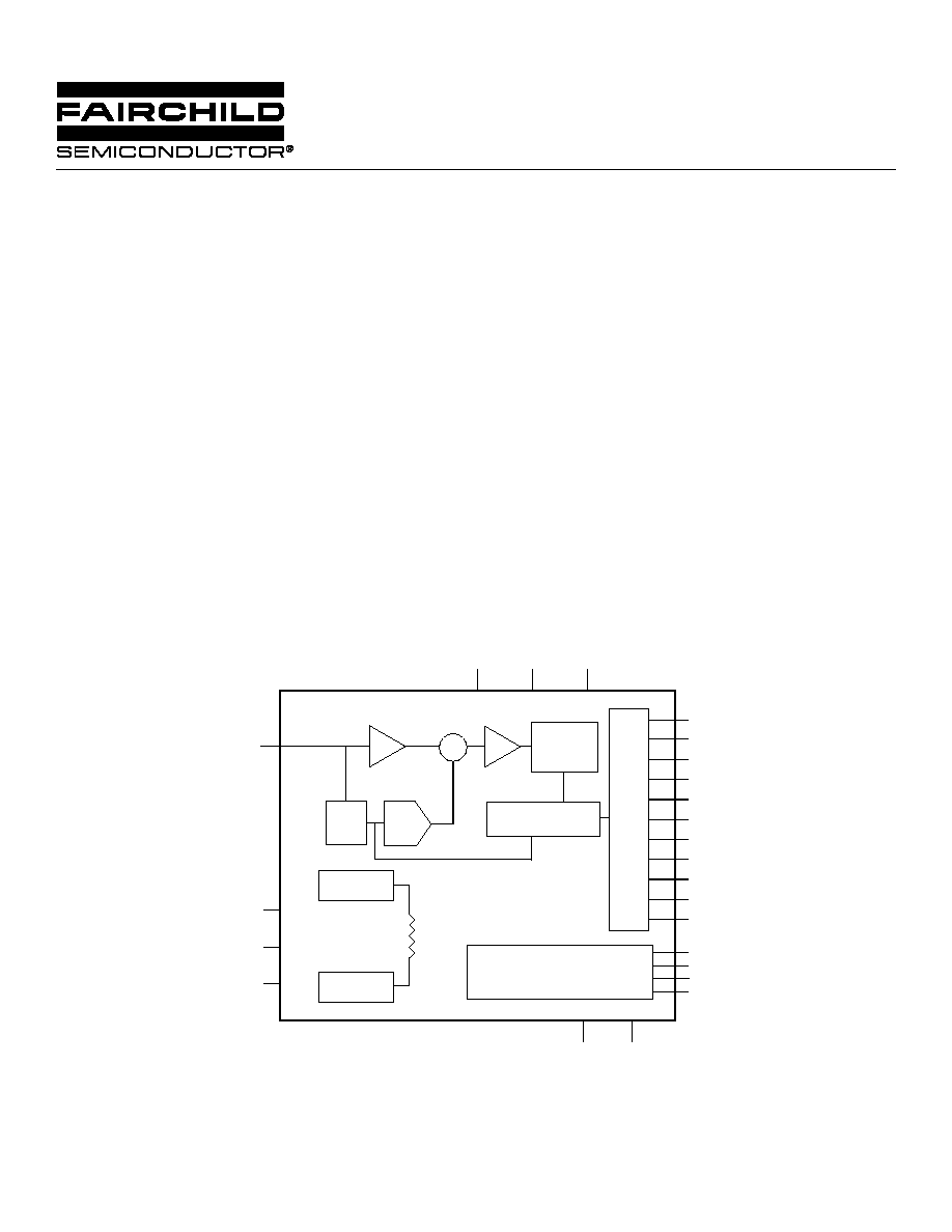
BLOCK DIAGRAM
NCLK (ECL)
Analog Input
AVCC
CLK (ECL)
Timing and
Control
8-Bit Folder
ADC
(LSB)
T/H
3-Bit
Flash
(MSB)
3-Bit
DAC
Error Correction Logic
T/H
Output
Latches
and
Buffers
(TTL)
D4
D3
D2
D1
D0
D9 (MSB)
D8
D7
D6
D5
D10 (Overrange)
MINV (CMOS/TTL)
LINV (CMOS/TTL)
VEE
AGND
DGND
VIN
DVCC
Internal
+1.0 V Reference
Internal
-1.0 V Reference
Reference
Ladder
VT
*
VM
*
VB
*
*
Provided for reference decoupling purposes only.
APPLICATIONS
∑ Professional Video
∑ HDTV
∑ Communications
∑ Imaging
∑ Digital Oscilloscopes
FEATURES
∑ 10-Bit, 100 MSPS Analog-to-Digital Converter
∑ Monolithic Bipolar
∑ Single-Ended Bipolar Analog Input
∑ -1.0 V to +1.0 V Analog Input Range
∑ Internal Sample-and-Hold
∑ Internal Voltage Reference
∑ Programmable Data Output Formats
∑ Single Ended TTL Outputs
∑ Differential ECL Clock Input
GENERAL DESCRIPTION
The SPT7871 is a 10-bit, 100 MSPS analog-to-digital con-
verter, with a two stage subranging flash/folder architecture.
The bipolar, single-ended analog input provides an easy
interface for most applications. Programmable data output
formats provide additional ease of implementation and flex-
ibility. The device supports high speed TTL outputs.
The resolution and performance of this device makes it well
suited for professional video and HDTV applications. The on-
chip track-and-hold provides for excellent AC performance
enabling this device to be a converter of choice for RF
communications and digital sampling oscilloscopes. The
SPT7871 is available in a 44L cerquad package in the
industrial temperature range and in die form.

2
9 / 7 / 9 8
SPT7871
ABSOLUTE MAXIMUM RATING (Beyond which damage may occur)
1
Supply Voltages
AV
CC ........................................................................
0 to +6.5 V
DV
CC ........................................................................
0 to +6.5 V
V
EE .............................................................................
0 to -6.5 V
Input Voltages
Analog Input ............................................. V
EE
V
IN
V
CC
LINV/MINV Inputs .......................... -0.5 V to V
CC
+0.5 V
CLK/NCLK Inputs ........................................... V
EE
to 0 V
Output
Digital Outputs ......................................... +30 to -30 mA
Temperature
Operating Temperature ............................. -40 to + 85
∞
C
Junction Temperature ........................................ + 175
∞
C
Lead, Soldering (10 seconds) ............................ + 300
∞
C
Storage .................................................... -60 to + 150
∞
C
Note: 1. Operation at any Absolute Maximum Ratings is not implied. See Electrical Specifications for proper nominal applied
conditions in typical applications.
DC Performance
Resolution
10
Bits
Differential Linearity
f
Clock
= 6.4 MHz
I
-1.0
±
0.5
±
1.25
LSB
Integral Linearity, Best Fit
f
Clock
= 6.4 MHz
I
±
1.0
±
2.0
LSB
Full Temperature
V
±
2.5
LSB
No Missing Codes
f
Clock
= 6.4 MHz
I
Guaranteed
Analog Input
Input Voltage Range
V
±
1.0
V
Input Bias Current
I
-100
25
100
µ
A
Input Resistance
I
50
150
k
Full Temperature
V
100
k
Input Capacitance
V
5
pF
Input Bandwidth
Full Power
IV
150
180
MHz
±
FS Offset Error
I
±
20
±
100
mV
Timing Characteristics
Minimum Conversion Rate
V
2
MSPS
Maximum Conversion Rate
IV
100
MSPS
Pipeline Delay (Latency)
IV
2
Clock
Transient Response
V
10
ns
Overvoltage Recovery Time
V
10
ns
Output Delay (t
d
)
V
3
ns
Aperture Delay Time
V
1
ns
Aperture Jitter Time
V
5
ps (rms)
Dynamic Performance
Effective Number of Bits
f
IN
= 10 MHz
I
8.1
8.5
Bits
f
IN
= 25 MHz
I
8.1
8.5
Bits
f
IN
= 25 MHz
f
clock
= 100 MHz
V
8.0
Bits
f
IN
= 50 MHz
I
7.5
7.8
Bits
f
IN
= 50 MHz
f
clock
= 100 MHz
V
7.5
Bits
Signal-To-Noise Ratio
f
IN
= 10 MHz
I
52
54
dB
f
IN
= 25 MHz
I
52
54
dB
f
IN
= 25 MHz
f
clock
= 100 MHz
V
51
dB
f
IN
= 50 MHz
I
52
54
dB
f
IN
= 50 MHz
f
clock
= 100 MHz
V
50
dB
Total Harmonic Distortion
1
f
IN
= 10 MHz
I
-56
-62
dBc
f
IN
= 25 MHz
I
-56
-60
dBc
f
IN
= 25 MHz
f
clock
= 100 MHz
V
-56
dBc
f
IN
= 50 MHz
I
-48
-51
dBc
f
IN
= 50 MHz
f
clock
= 100 MHz
V
-50
dBc
T
A
= +25
∞
C , DV
CC
=AV
CC
= +5.0 V, V
EE
= -5.2 V, V
IN
=
±
1.0 V, f
clock
= 80 MHz, 50% clock duty cycle, unless otherwise specified.
TEST
TEST
PARAMETERS
CONDITIONS
LEVEL
MIN
TYP
MAX
UNITS
ELECTRICAL SPECIFICATIONS

3
9 / 7 / 9 8
SPT7871
ELECTRICAL SPECIFICATIONS
T
A
= +25
∞
C , DV
CC
=AV
CC
= +5.0 V, V
EE
= -5.2 V, V
IN
=
±
1.0 V, f
clock
= 80 MHz, 50% clock duty cycle, unless otherwise specified.
TEST
TEST
PARAMETERS
CONDITIONS
LEVEL
MIN
TYP
MAX
UNITS
Dynamic Performance
Signal-to-Noise + Distortion (SINAD)
f
IN
=10 MHz
I
51
53
dB
f
IN
= 25 MHz
I
51
53
dB
f
IN
= 25 MHz
f
clock
= 100 MHz
V
50
dB
f
IN
= 50 MHz
I
47
49
dB
f
IN
= 50 MHz
f
clock
= 100 MHz
V
47
dB
Spurious Free Dynamic Range
f
IN
= 10 MHz
V
65
dB FS
f
IN
= 25 MHz
V
63
dB FS
f
IN
= 50 MHz
V
52
dB FS
Two-Tone IMD Rejection
2
V
-65
dBc
Differential Phase
V
0.5
Degree
Differential Gain
V
1
%
Power Supply Requirements
AV
CC
Supply Voltage
IV
4.75
5.0
5.25
V
DV
CC
Supply Voltage
IV
4.75
5.0
5.25
V
V
EE
Supply Voltage
IV
-4.95
-5.2
-5.45
V
V
CC
Supply Current
Full Temperature
VI
210
248
mA
V
EE
Supply Current
Full Temperature
VI
128
151
mA
Power Dissipation
Full Temperature
VI
1.7
2.0
W
Power Supply Rejection Ratio
IV
30
dB
Digital Inputs
LINV, MINV
V
CMOS/TTL
Logic
Clock Inputs
Logic 1 Voltage (ECL)
VI
-1.1
V
Logic 0 Voltage (ECL)
VI
-1.5
V
Maximum Input Current Low
VI
-100
+100
µ
A
Maximum Input Current High
VI
-100
+100
µ
A
Pulse Width Low (CLK)
IV
4.0
250
ns
Pulse Width High (CLK)
IV
4.0
250
ns
Rise/Fall Time
20% to 80%
IV
1.5
ns
Digital Outputs
Logic 1 Voltage (TTL)
2 mA
VI
2.4
2.8
V
Logic 0 Voltage (TTL)
2 mA
VI
0.5
0.8
V
t
Rise
10% to 90%
V
2.0
ns
t
Fall
10% to 90%
V
2.0
ns
1
2048 pt FFT using distortion harmonics 2 through 10.
2
Measured as a second order (f1-f2) intermodulation product from a two-tone test with each input tone at 0 dBm.
TEST LEVEL CODES
All electrical characteristics are subject to the
following conditions:
All parameters having min/max specifications
are guaranteed. The Test Level column indi-
cates the specific device testing actually per-
formed during production and Quality Assur-
ance inspection. Any blank section in the data
column indicates that the specification is not
tested at the specified condition.
Unless otherwise noted, all tests are pulsed
tests; therefore, T
J
= T
C
= T
A
.
TEST PROCEDURE
100% production tested at the specified temperature.
100% production tested at T
A
= +25
∞
C, and sample
tested at the specified temperatures.
QA sample tested only at the specified temperatures.
Parameter is guaranteed (but not tested) by design
and characterization data.
Parameter is a typical value for information purposes
only.
100% production tested at T
A
= +25
∞
C. Parameter is
guaranteed over specified temperature range.
TEST LEVEL
I
II
III
IV
V
VI
4
9 / 7 / 9 8
SPT7871
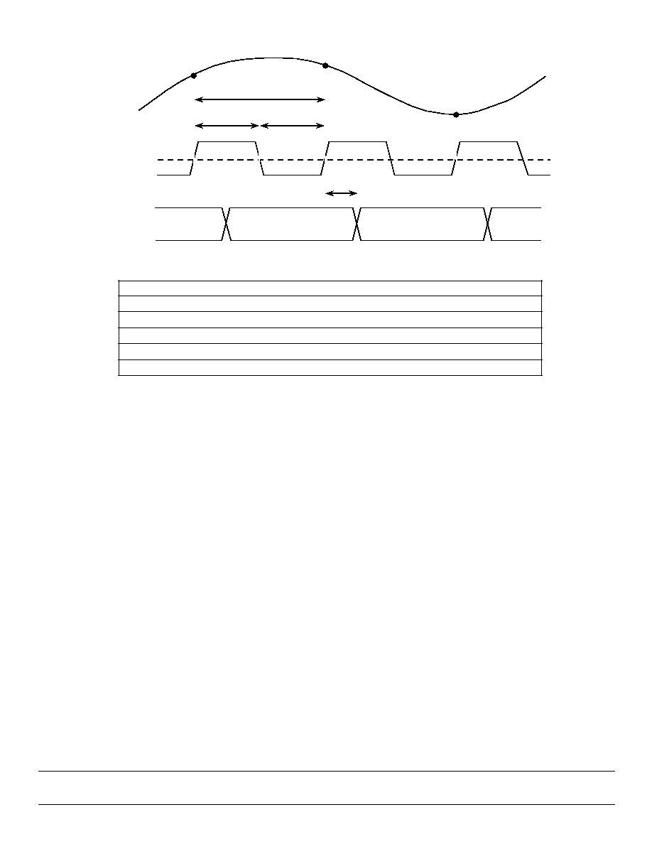
Figure 1 - Timing Diagram
THEORY OF OPERATION
The SPT7871 uses a two stage subranging architecture
incorporating a 3-bit flash MSB conversion stage followed by
an 8-bit interpolating folder conversion stage. Digital error
correction logic combines the results of both stages to pro-
duce a 10-bit data conversion digital output.
The analog signal is input directly to the 3-bit flash converter
which performs a 3-bit conversion and in turn drives an
internal DAC used to set the second stage voltage reference
level. The 3-bit result from the flash conversion is input to the
digital error correction logic and used in calculation of the
upper most significant bits of the data output.
The analog input is also input directly to an internal track-and-
hold amplifier. The signal is held and amplified for use in the
second stage conversion. The output of the track-and-hold is
input into a summing junction that takes the difference
between the track-and-hold amplifier and the 3-bit DAC
output. The residual is captured by a second track-and-hold
which holds and amplifies this residual voltage.
The residual held by the track-and-hold amplifier is input to an
8-bit interpolating folder stage for data conversion. The 8-bit
converted data from the folder stage is input into the digital
error correction logic and used in calculation of the lower
significant bits.
The error correction logic incorporates a proprietary scheme
for compensation of any internal offset and gain errors that
might exist to determine the 10-bit conversion result. The
resultant 10-bit data conversion is internally latched and
presented on the data output pins via buffered output drivers.
TYPICAL INTERFACE CIRCUIT
The SPT7871 requires few external components to achieve
the stated operation and performance. Figure 2 shows the
typical interface requirements when using the SPT7871 in
normal circuit operation. The following section is a description
of the pin functions and outlines critical performance criteria
to consider for achieving the optimal device performance.
POWER SUPPLIES AND GROUNDING
The SPT7871 requires the use of three supply voltages: V
EE,
AV
CC
and DV
CC
. The V
EE
and AV
CC
supplies should be
treated as analog supply sources. This means the V
EE
and
V
CC
ground returns of the device should both be connected
to the analog ground plane. Each power supply pin should be
bypassed as closely as possible to the device with .01
µ
F and
2.2
µ
F capacitors as shown in figure 2.
The two grounds available on the SPT7871 are AGND and
DGND. DGND is used only for TTL outputs and is to be
referenced to the output pullup voltage. These grounds are
not tied together internal to the device. The use of ground
planes is recommended to achieve the best performance of
the SPT7871. The AGND and the DGND ground planes
should be separated from each other and only connected
together at the device through an inductance or ferrite bead.
Doing this will minimize the ground noise pickup.
Table I - Data Output Timing Parameters
Timing Parameter
Minimum
Typical
Maximum
f
clock
2 MHz
100 MHz
Clock Pulse Width High (t
pwh
)
4.0 ns
250 ns
Clock Pulse Width Low (t
pwl
)
4.0 ns
250 ns
Switching Delay (t
d
)
3 ns
Clock Latency
2 clock cycles
CLK
OUTPUT
DATA
t
d
DATA VALID
N
N
N+1
N+2
DATA VALID
N-1
N-3
N-2
tclk
tpwh
tpwl

5
9 / 7 / 9 8
SPT7871
available and are controlled by the MINV and LINV pins.
Table III shows the four possible output formats possible as
a function of MINV and LINV. Table II shows the output coding
data format versus analog input voltage relationship.
Table II - Output Coding Data Format
V
IN
D10
D9...D0 (Binary*)
D9...D0 (2's Comp*)
>+1.0 V
1
11 1111 1111
01 1111 1111
(+FS)
0
11 1111 1111
01 1111 1111
+1.0 V -1 LSB
0
11 1111 1110
01 1111 1110
0.0 V
0
10 0000 0000
00 0000 0000
0
01 1111 1111
11 1111 1111
-1.0 V +1 LSB
0
00 0000 0001
10 0000 0001
(-FS)
0
00 0000 0000
10 0000 0000
<-1.0 V
0
00 0000 0000
10 0000 0000
*Refer to table III for possible output formats.
OVERRANGE BIT - D10
D10 is the overrange bit which is asserted whenever the
analog input signal exceeds the positive full scale input by
1 LSB. When this condition occurs the D10 bit will be asserted
to logic high and remain high continuously until the overrange
condition is removed from the input.
All other output signals will also stay at their maximum
encoded output throughout this condition. D10 is not as-
serted for an underscale condition when the input exceeds
the negative full scale.
DIGITAL OUTPUT DATA TIMING
The data is presented on the output pins two clock cycles after
the input is sampled with an additional output delay of
typically 3 ns. The data is held valid for one clock cycle. Refer
to the timing diagram shown in figure 1.
DIGITAL OUTPUT CONTROL PINS - MINV, LINV
Two digital output control pins control the digital output
format. See table III. The MINV pin is a CMOS/TTL-compat-
ible input. It inverts the most-significant bit (D9) when tied to
+5 V. The most-significant bit (D9) is noninverted when MINV
is tied to ground or floated. The MINV pin is internally pulled
down to ground.
The LINV pin is a CMOS/TTL-compatible input. It inverts the
least-significant bits (D8 through D0) when tied to +5 V. The
least-significant bits (D8 through D0) are noninverted when
LINV is tied to ground or floated. The LINV pin is internally
pulled down to ground.
Table III - Data Output Bits
MINV
LINV
Description of Data
0 V
0 V
Binary (Noninverted)
0 V
+5 V
Two's Complement (Inverted)
+5 V
0 V
Two's Complement (Noninverted)
+5 V
+5 V
Binary (Inverted)
ANALOG INPUT
The SPT7871 has a single-ended analog input with a bipolar
input range from -1 V to +1 V. The bipolar input allows for
easier interface by external op amps when compared to
unipolar input devices. Because the input common mode is
0 V, the external op amp can operate without a voltage offset
on the output, thereby maximizing op amp head room and
minimizing distortion.
In addition, the 0 V common mode allows for a very simple DC
coupled analog input connection if desired. The current drive
requirements for the analog input are minimal when com-
pared to conventional flash converters due to the SPT7871's
low input capacitance of only 5 pF and very high input
impedance of 150 k
.
CLOCK INPUTS
The clock inputs are designed to be driven differentially
with ECL levels. For optimal noise performance, the clock
input rise time should be a maximum of 1.5 ns. Because of
this, the use of
fast logic is recommended. The analog input
signal is latched on the rising edge of the CLK.
The clock may be driven single-ended since the NCLK pin is
internally biased to -1.3 V. NCLK may be left open but a
.01
µ
F bypass capacitor from NCLK to AGND is recom-
mended. NOTE: System performance may be degraded due
to increased clock noise or jitter.
The performance of the SPT7871 is specified and tested with
a 50% clock duty cycle. However, at sample rates greater
than 80 MSPS, additional gains in the dynamic performance
of the device may be obtained by adjusting the clock duty
cycle. Typically, operation near 55% duty cycle will yield
improved results.
INTERNAL VOLTAGE REFERENCE
The SPT7871 incorporates an on-chip voltage reference.
The top and bottom reference voltages are each internally
tied to their respective top and bottom of the internal refer-
ence ladder. The pins for the voltage references and the
ladder (including the center of the ladder) are brought out to
pins on the device for decoupling purposes only (pins V
T,
V
M,
and V
B
). A .01
µ
F capacitor should be used on each pin and
tied to AGND. See the typical interface circuit (figure 2).
The internal voltage reference and the internal error correc-
tion logic eliminate the need for driving externally the voltage
reference ladder. In fact,
the voltage reference ladder should
not be driven with an external voltage reference source as the
internal error correction circuitry already compensates for the
internal voltage and no improvement will result.
DIGITAL OUTPUTS
DIGITAL OUTPUT DATA FORMAT - D0 - D9
D0 is the least-significant bit for the digital data output, and D9
is the most-significant bit. Four data output formats are