SPT7935
12-BIT, 20 MSPS, 79 mW A/D CONVERTER
FEATURES
∑ 12-Bit, 20 MSPS Analog-to-Digital Converter
∑ Monolithic CMOS
∑ Internal Track-and-Hold
∑ Low Input Capacitance: 1.4 pF
∑ Low Power Dissipation: 79 mW
∑ 2.8 ≠ 3.6 V Power Supply Range
∑ TTL-Compatible Outputs
APPLICATIONS
∑ CCD Imaging Cameras and Sensors
∑ Medical Imaging
∑ RF Communications
∑ Document and Film Scanners
∑ Electro-Optics
∑ Transient Signal Analysis
∑ Handheld Equipment
GENERAL DESCRIPTION
The SPT7935 12-bit, 20 MSPS analog-to-digital converter
has a pipelined converter architecture built in a CMOS
process. It delivers high performance with a typical power
dissipation of only 79 mW. With low distortion and high
dynamic range, this device offers the performance needed
for imaging, multimedia, telecommunications and instrumen-
tation applications.
The SPT7935 is available in a 44-lead Thin Quad Flat Pack
(TQFP) package in the industrial temperature range (≠40 to
+85
∞
C).
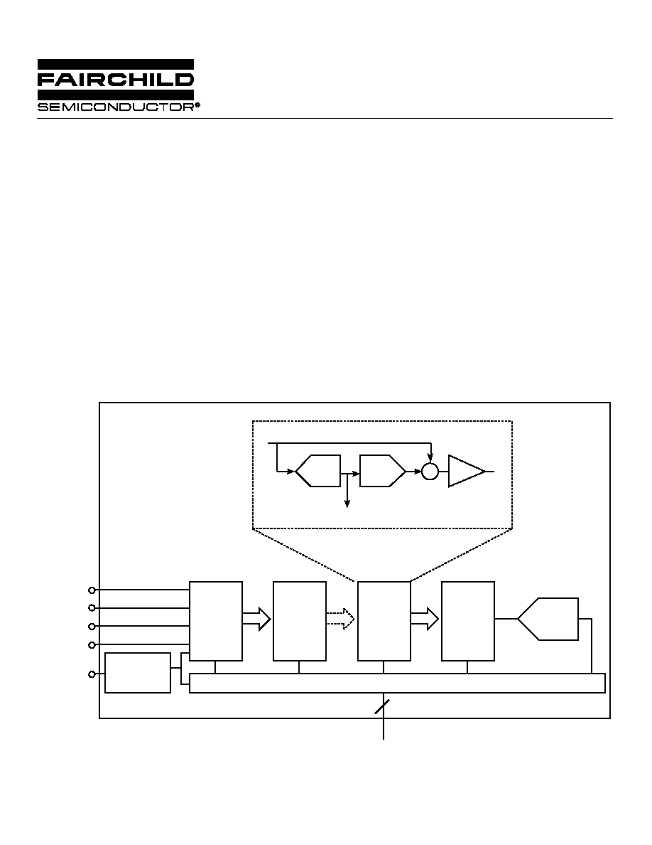
BLOCK DIAGRAM
Stage
1
Stage
2
Stage
9
Stage
10
2-Bit
ADC
Clock
Driver
Digital Delays, Error Correction and Output
V
IN
+
V
IN
≠
V
REF
+
V
REF
≠
CLK
Digital Output (D0 ≠ D11)
12
DAC
ADC
+
G=2
≠
D<1...0> Pipeline Stage

2
7 / 1 2 / 0 0
SPT7935
ELECTRICAL SPECIFICATIONS
T
A
=T
MIN
≠T
MAX
, V
DD1
=V
DD2
=V
DD3
=
3.3 V,
V
REF
≠=1.0 V, V
REF
+=2.0 V, Common Mode Voltage=1.65 V,
CLK
=20 MSPS, Bias 1=90
µ
A,
Bias 2=9.5
µ
A, Differential Input, Duty Cycle=50%, unless otherwise specified.
TEST
TEST
SPT7935
PARAMETERS
CONDITIONS
LEVEL
MIN
TYP
MAX
UNITS
DC Accuracy
Resolution
12
Bits
Differential Linearity
V
±
0.6
LSB
Integral Linearity
V
±
3.0
LSB
No Missing Codes
VI
Guaranteed
Analog Input
Input Voltage Range (Differential)
IV
±
0.6
±
1.0
±
1.7
V
Common Mode Input Voltage
IV
1.2
1.65
1.9
V
Input Capacitance
V
1.4
pF
Input Bandwidth (Large Signal)
V
120
MHz
Offset (Mid-scale)
V
IN
+=V
IN
≠=V
CM
V
±
1.0
% FSR
Gain Error
V
0.3
% FSR
Reference Voltages
Reference Input Voltage Range
IV
0.6
1.0
1.7
V
(V
REF
+ ≠ V
REF
≠)
Negative Reference Voltage (V
REF
≠)
IV
0.9
1.0
1.3
V
Positive Reference Voltage (V
REF
+)
IV
1.9
2.0
2.6
V
Common Mode Output Voltage (V
CM
)
I
O
= ≠1
µ
A
VI
1.3
1.65
1.8
V
V
REF
+ Current
V
35
µ
A
V
REF
≠ Current
V
≠25
µ
A
Switching Performance
Maximum Conversion Rate
VI
20
MHz
Pipeline Delay
IV
7.5
Clocks
(See Timing Diagram)
Aperture Delay Time (T
AP
)
V
5
ns
Aperture Jitter Time
V
10
ps-rms
Dynamic Performance
Effective Number of Bits
IN
= 5.0 MHz
VI
9.2
9.8
Bits
IN
= 10.0 MHz
V
9.0
Bits
Signal-To-Noise Ratio
IN
= 5.0 MHz
VI
59
62
dB
IN
= 10.0 MHz
V
58
dB
Total Harmonic Distortion
IN
= 5.0 MHz
VI
≠68
≠61
dB
IN
= 10.0 MHz
V
≠60
dB
ABSOLUTE MAXIMUM RATINGS (Beyond which damage may occur)
1
25
∞
C
Supply Voltages
V
DD1 ....................................................................
≠0.5 V to +6 V
V
DD2 ....................................................................
≠0.5 V to +6 V
V
DD3 ....................................................................
≠0.5 V to +6 V
Input Voltages
Analog Input ................................. ≠0.5 V to (V
DD
+0.5 V)
Digital Input .................................. ≠0.5 V to (V
DD
+0.5 V)
V
REF
+ .......................................... ≠0.5 V to (V
DD
+0.5 V)
V
REF
≠ .......................................... ≠0.5 V to (V
DD
+0.5 V)
CLK .............................................. ≠0.5 V to (V
DD
+0.5 V)
Temperature
Operating Temperature ............................. ≠40 to +85
∞
C
Storage Temperature ............................... ≠65 to +125
∞
C
Note: 1. Operation at any Absolute Maximum Rating is not
implied. See Electrical Specifications for proper
nominal applied conditions in typical applications.

3
7 / 1 2 / 0 0
SPT7935
TEST LEVEL
I
II
III
IV
V
VI
TEST PROCEDURE
100% production tested at the specified temperature.
100% production tested at T
A
= +25
∞
C, and sample tested at
the specified temperatures.
QA sample tested only at the specified temperatures.
Parameter is guaranteed (but not tested) by design and
characterization data.
Parameter is a typical value for information purposes only.
100% production tested at T
A
= +25
∞
C. Parameter is guaran-
teed over specified temperature range.
TEST LEVEL CODES
All electrical characteristics are subject to the
following conditions: All parameters having
min/max specifications are guaranteed. The
Test Level column indicates the specific
device testing actually performed during pro-
duction and Quality Assurance inspection.
Any blank section in the data column indi-
cates that the specification is not tested at the
specified condition.
ELECTRICAL SPECIFICATIONS
T
A
=T
MIN
≠T
MAX
, V
DD1
=V
DD2
=V
DD3
=
3.3 V,
V
REF
≠=1.0 V, V
REF
+=2.0 V, Common Mode Voltage=1.65 V,
CLK
=20 MSPS, Bias 1=90
µ
A,
Bias 2=9.5
µ
A, Differential Input, Duty Cycle=50%, unless otherwise specified.
TEST
TEST
SPT7935
PARAMETERS
CONDITIONS
LEVEL
MIN
TYP
MAX
UNITS
Dynamic Performance≠Continued
Signal-To-Noise and Distortion
IN
= 5 MHz
VI
57
61
dB
IN
= 10 MHz
V
56
dB
Spurious Free Dynamic Range
IN
= 5.0 MHz
VI
62
70
dB
IN
= 10.0 MHz
V
61
dB
Differential Phase
V
0.2
Degrees
Differential Gain
V
0.5
%
Digital Inputs
Logic 1 Voltage
VI
80% V
DD
Logic 0 Voltage
VI
20% V
DD
Maximum Input Current Low
V
IN
= GND
VI
±
1
µ
A
Maximum Input Current High
V
IN
= V
DD
VI
±
1
µ
A
Input Capacitance
V
1.8
pF
Digital Outputs
Logic 1 Voltage
I
O
= -2 mA
VI
85% V
DD
95% V
DD
V
Logic 0 Voltage
I
O
= +2 mA
VI
0.1
0.4
V
CLK to Output Delay Time (t
D
)
IV
4
8
12
ns
Power Supply Requirements
Supply Voltages
V
DD1
, V
DD2
, V
DD3
IV
2.8
3.3
3.6
V
Supply Current
I
DD
VI
24
30
mA
Power Dissipation
VI
79
100
mW
Power Supply Rejection Ratio (PSRR)
V
67
dB
4
7 / 1 2 / 0 0
SPT7935
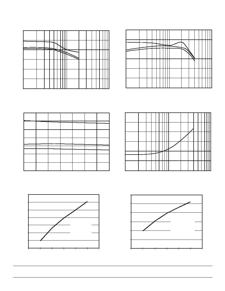
THD
SNR
SINAD
THD, SNR, SINAD (dB)
20
30
40
50
60
70
80
100
101
102
THD, SNR, SINAD vs Input Frequency
Input Frequency (MHz)
SNR
THD
SINAD
SNR
THD
SINAD
THD, SNR, SINAD (dB)
20
30
40
50
60
70
80
10 0
101
102
THD, SNR, SINAD vs Sample Rate
Sample Rate (MSPS)
Note: Bias1 and Bias2 currents optimized for each sample rate.
56
58
60
62
64
66
68
70
0
25
70
Temperature (∞C)
THD, SNR, SINAD (dB)
THD, SNR, SINAD vs Temperature
THD
SNR
SINAD
Power Dissipation (mW)
0
25
50
75
100
125
150
10 0
101
102
Power Dissipation vs Sample Rate
Sample Rate (MSPS)
Note: Bias1 and Bias2 optimized for each sample rate.
Bias 2 Voltage vs Bias 2 Current
0.60
0.65
0.70
0.75
0.80
0.85
0.90
0
3
6
9
12
15
18
IBias2 (
µ
A)
VBias2 (V)
IBias2
VBias2
3
0.6975
6
0.7535
9
0.796
12
0.8295
15
0.8595
Bias 1 Voltage vs Bias 1 Current
2.0
2.2
2.4
2.6
2.8
3.0
3.2
3.4
0
30
60
90
120
150
180
IBias1 (
µ
A)
VBias1 (V)
IBias1 VBias1
30
2.19
60
2.53
90
2.79
120
3.00
150
3.22
TYPICAL PERFORMANCE CHARACTERISTICS
5
7 / 1 2 / 0 0
SPT7935
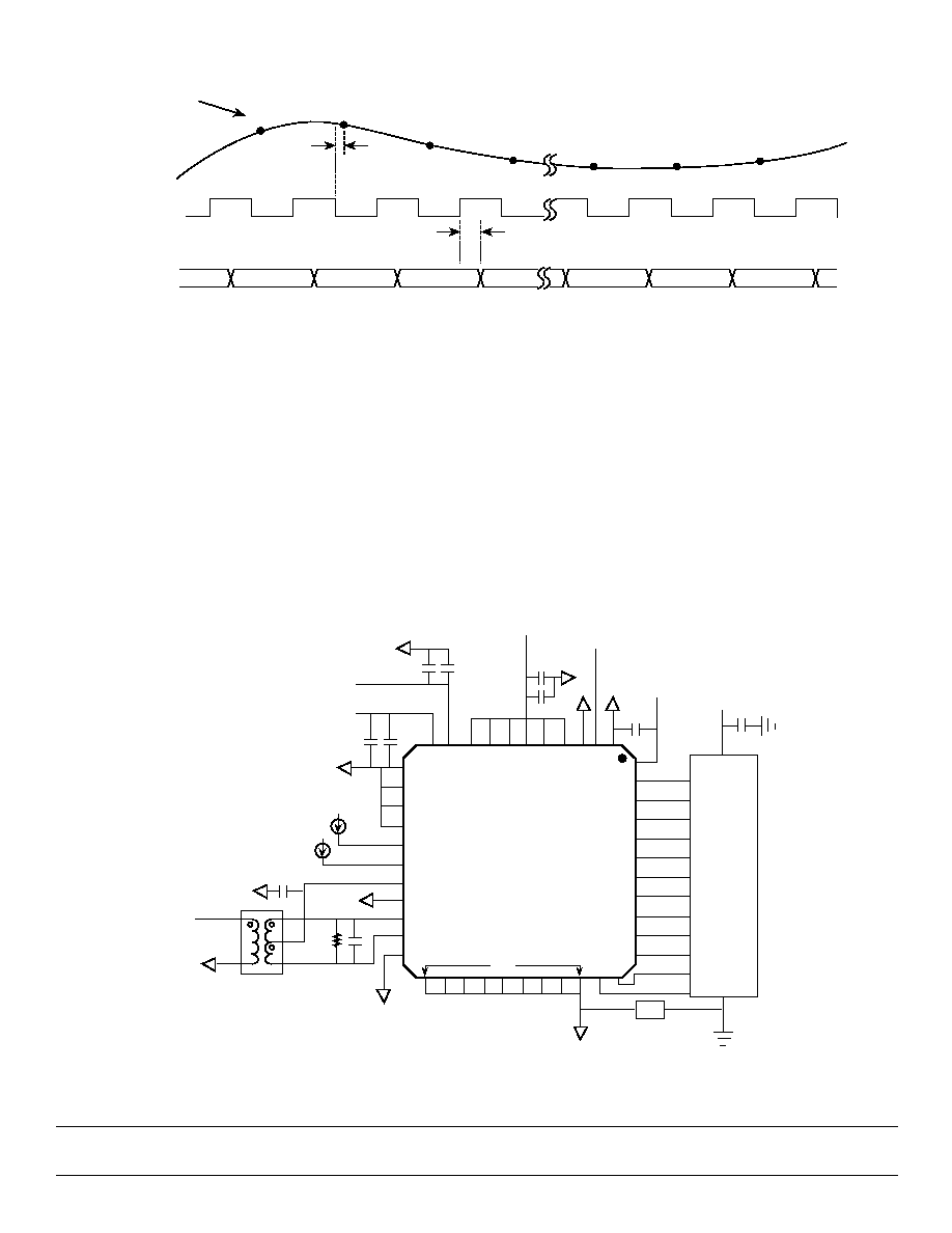
Figure 1 ≠ Timing Diagram
N+8
N+7
N+6
N+2
N+1
N
N-1
t
D
N-2
N-1
N
Sampling Points
t
AP
A
IN
CLK
D
OUT
GENERAL DESCRIPTION
The SPT7935 is an ultra-low power, 12-bit, 20 MSPS ADC.
It has a pipelined architecture and incorporates digital error
correction of the 11 most significant bits. This error correction
ensures good linearity performance for input frequencies up
to Nyquist. The inputs are fully differential, making the device
insensitive to system-level noise. This device can also be
used in a single-ended mode. (See analog input section.)
With the power dissipation roughly proportional to the sam-
pling rate, this device is ideal for very low power applications
in the range of 1 to 20 MSPS.
TYPICAL INTERFACE CIRCUIT
The SPT7935 requires few external components to achieve
the stated operation and performance. Figure 2 shows the
typical interface requirements when using the SPT7935 in
normal circuit operation. The following sections provide
a description of the functions and outline critical perform-
ance criteria to consider for achieving the optimal device
performance.
ANALOG INPUT
The input of the SPT7935 can be configured in various ways
depending on if a single-ended or differential, AC- or DC-
coupled input is desired.
Figure 2 ≠ Typical Interface Circuit
GND
.01
µ
F
+
4.7
µ
F
Ref≠ In
(+1.15 V)
Ref+ In
(+2.15 V)
.01
µ
F
+
10
µ
F
0.1
µ
F
+3.3 V
CLK In
(3 V Logic)
Interfacing
3 V Logic
Decoupling Cap
+3.3 V
DGND
FB
(MSB)
AGND
U1
SPT7935
.01
µ
F
(+1.65 V)
Minicircuit
T1-6T
RF In
51
68 pF
22
23
11
12
34
33
1
44
(LSB)
N/C
N/C
N/C
GND
Bias1
Bias2
V
CM
GND
V
IN
+
V
IN
≠
GND
D11
D10
V
DD3
D0
D1
D2
D3
D4
D5
D6
D7
D8
D9
GND
CLK
N/C
V
DD3
V
DD2
V
DD2
V
DD1
V
DD1
V
DD1
V
REF
≠
V
REF
+
.01
µ
F
+
4.7
µ
F
+3.3 V Digital
9.5
µ
A
90
µ
A
Notes: All V
DD1
, V
DD2
and V
DD3
should be tied together.
FB = Ferrite Bead; must be placed as close to U1 as possible.