SPT7936
12-BIT, 28 MSPS SAMPLING A/D CONVERTER
FEATURES
∑ 3.0-3.6 V Power Supply
∑ Typical SINAD: 60 dB for (f
IN
= 10 MHz)
∑ Low power: (260 mW @3.3 V)
∑ Sample Rate: 28 MSPS
∑ Internal Sample/Hold
∑ Differential Input
∑ Sleep Mode (Power Down)
APPLICATIONS
∑ Imaging
∑ Test Equipment
∑ Computer Scanners
∑ Communications
∑ Set-Top Boxes
GENERAL DESCRIPTION
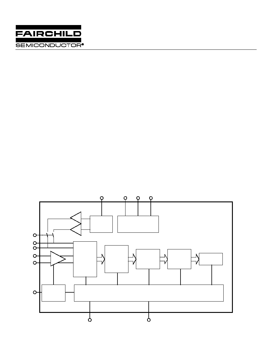
The SPT7936 is a compact, high-speed, low power 12-bit
monolithic analog-to-digital converter, implemented in a
0.5
µ
m CMOS process. The converter includes sample and
hold. The full scale range can be set between
±
0.6 V and
±
1.2
V using external references. It operates from a single 3.0-3.6
V supply-compatible with modern digital systems. Most con-
verters in this performance range demand at least a +5 V
supply. Its low distortion and high dynamic range offers the
performance needed for demanding imaging, multimedia,
telecommunications and instrumentation applications.
The SPT7936 has a pipelined architecture - resulting in low
input capacitance. Digital error correction of the 11 most
significant bits ensures good linearity for input frequencies
approaching Nyquist.
The device is available in a 44L TQFP package over the
commercial temperature range of 0 to +70
∞
C.
Digital Delays, Error Correction and Output Register
Ref Buff
Ref Buff
BGREF
BIAS CELL
Bias 0 Bias 1
CM
Ext Ref
THA
Clock
Driver
VREF+
VREF-
VIN+
VIN-
Clock
Stage 1
Stage 2
Stage 3
Stage 10
Stage_Last
(2-Bit Flash)
OR
Bit <11...0)
BGAP
BLOCK DIAGRAM

2
8 / 1 / 0 0
SPT7936
ABSOLUTE MAXIMUM RATINGS (Beyond which damage may occur)
1
25
∞
C
Supply Voltages
V
DD1 ...................................................................
- 0.3 V to +6 V
V
DD2 ...................................................................
- 0.3 V to +6 V
Input Voltages
Analog In ....................................... - 0.3 V to V
DD
+ 0.3 V
Digital In ........................................ - 0.3 V to V
DD
+ 0.3 V
REF
P ....................................................
- 0.3 V to V
DD
+ 0.3 V
REF
N ....................................................
- 0.3 V to V
DD
+ 0.3 V
CLOCK .......................................... - 0.3 V to V
DD
+ 0.3 V
Temperatures
Operating Temperature ................................. 0 to +70
∞
C
Storage Temperature.. ............................. - 65 to +125
∞
C
Note:
1.
Operation at any Absolute Maximum Rating is not implied. See Electrical Specifications for proper nominal
applied conditions in typical applications.
ELECTRICAL SPECIFICATIONS
T
A
= T
MIN
-T
MAX
, V
DD1
=V
DD2
= 3.3 V, Sampling Rate = 28 MSPS, Differential input signal, 50% duty cycle clock with 2.5 ns rise and fall times, unless otherwise
specified.
TEST
TEST
SPT7936
PARAMETERS
CONDITIONS
LEVEL
MIN
TYP
MAX
UNITS
DC Accuracy
Differential Nonlinearity (DNL)
VI
±
0.5
±
1.0
LSB
Integral Nonlinearity
VI
±
1.3
±
3.0
LSB
Common Mode Rejection Ratio (CMRR)
V
54
dB
No Missing Codes
Guaranteed
Analog Input
Input Voltage Range (differential) VFSR
IV
0.6
±
1
±
1.2
V
Common Mode Input Voltage VCMI
IV
1.2
1.5
1.6
V
Input Capacitance C
IN
V
2
pF
(From Each Input to Ground)
Midscale Offset V
OS
V
IN
+=V
IN
≠=V
CM
V
±
2
%
Gain Error
V
-0.2
%
Input Bandwidth
Large Signal
V
150
MHz
Reference Voltages
Internal Reference Voltage on Pin 10 (V
REFNI
)
VI
0.95
1.0
1.05
V
Internal Reference Voltage on Pin 11 (V
REFPI
)
VI
1.95
2.0
2.05
V
Internal Reference Voltage Drift
IV
100
ppm/
∞
C
Negative Input Voltage (V
REF
-)
VI
0.9
1.0
1.3
V
Positive Input Voltage (V
REF
+)
VI
1.9
2.0
2.3
V
Reference Input Voltage Range (V
REF
+ -- V
REF
-)
IV
0.6
1.0
1.2
V
Common Mode Output Voltage (V
CM
)
VI
1.45
1.50
1.55
V
Bandgap Output Voltage (V
BGAP
)
VI
2.365
2.415
2.465
V
Dynamic Performance
Effective Number of Bits
f
IN
= 5.0 MHz
V
10.0
Bits
f
IN
= 10.0 MHz
VI
9.2
9.7
Bits
Signal to Noise and Distortion Ratio (SINAD)
f
IN
= 5.0 MHz
V
62
dB
f
IN
= 10.0 MHz
VI
57
60
dB
Signal to Noise Ratio (SNR)
f
IN
= 5.0 MHz
V
64
dB
Without Harmonics
f
IN
= 10.0 MHz
VI
59
63
dB
Total Harmonic Distortion (THD)
f
IN
= 5.0 MHz
V
≠66
dB
f
IN
= 10.0 MHz
VI
≠64
≠61
dB

3
8 / 1 / 0 0
SPT7936
ELECTRICAL SPECIFICATIONS
T
A
= T
MIN
-T
MAX
, V
DD1
=V
DD2
= 3.3 V, Sampling Rate = 28 MSPS, Differential input signal, 50% duty cycle clock with 2.5 ns rise and fall times, unless otherwise
specified.
TEST
TEST
SPT7936
PARAMETERS
CONDITIONS
LEVEL
MIN
TYP
MAX
UNITS
Dynamic Performance
Spurious Free Dynamic Range (SFDR)
f
IN
= 5.0 MHz
V
67
dB
f
IN
= 10.0 MHz
VI
62
64
dB
Differential Phase (DP)
V
0.08
degrees
Differential Gain (DG)
V
0.27
%
Digital Inputs
Logic 0 Voltage (V
IL
)
VI
20% V
DD
Logic 1 Voltage (V
IH
)
VI
80% V
DD
Logic 0 Current (IIL)
(V
I
=V
SS
)
VI
±
1
µ
A
Logic 1 Current (I
IH
)
(V
I
=V
DD
)
VI
±
1
µ
A
Input Capacitance (C
IND
)
V
1.8
pF
Digital Outputs
Logic 0 Voltage (V
OL
)
(I = +2 mA)
VI
0.2
0.4
V
Logic 1 Voltage (V
OH
)
(I = -2 mA)
VI
85% V
DD
90% V
DD
V
Output Hold Time (t
H
)
V
5
ns
Output Delay Time (t
D
)
V
8
ns
Switching Performance
Maximum Conversion Rate (f
S
)
VI
28
MSPS
Minimum Conversion Rate
IV
1
MSPS
Pipeline Delay (See Timing Diagram)
IV
8.0
Clocks
Aperture Jitter
AP
V
10
ps
Aperture Delay t
AP
V
2
ns
Power Supply
Supply Voltage V
DD
IV
3.0
3.3
3.6
V
Supply Current I
DD
ext ref
VI
75
87
mA
int ref
VI
79
91
mA
Power Dissipation P
D
ext ref
VI
248
288
mW
int ref
VI
260
300
mW
Sleep Mode Current
ext ref
VI
8
9
mA
int ref
VI
11
12
mA
Sleep Mode Power Dissipation
ext ref
VI
25
29
mW
int ref
VI
36
40
mW
Power Supply Rejection Ratio (PSRR)
V
52
dB
TEST LEVEL
I
II
III
IV
V
VI
TEST PROCEDURE
100% production tested at the specified temperature.
100% production tested at T
A
= +25
∞
C, and sample
tested at the specified temperatures.
QA sample tested only at the specified temperatures.
Parameter is guaranteed (but not tested) by design
and characterization data.
Parameter is a typical value for information purposes
only.
100% production tested at T
A
= +25
∞
C. Parameter is
guaranteed over specified temperature range.
TEST LEVEL CODES
All electrical characteristics are subject to the
following conditions: All parameters having min/
max specifications are guaranteed. The Test
Level column indicates the specific device test-
ing actually performed during production and
Quality Assurance inspection. Any blank sec-
tion in the data column indicates that the speci-
fication is not tested at the specified condition.
4
8 / 1 / 0 0
SPT7936
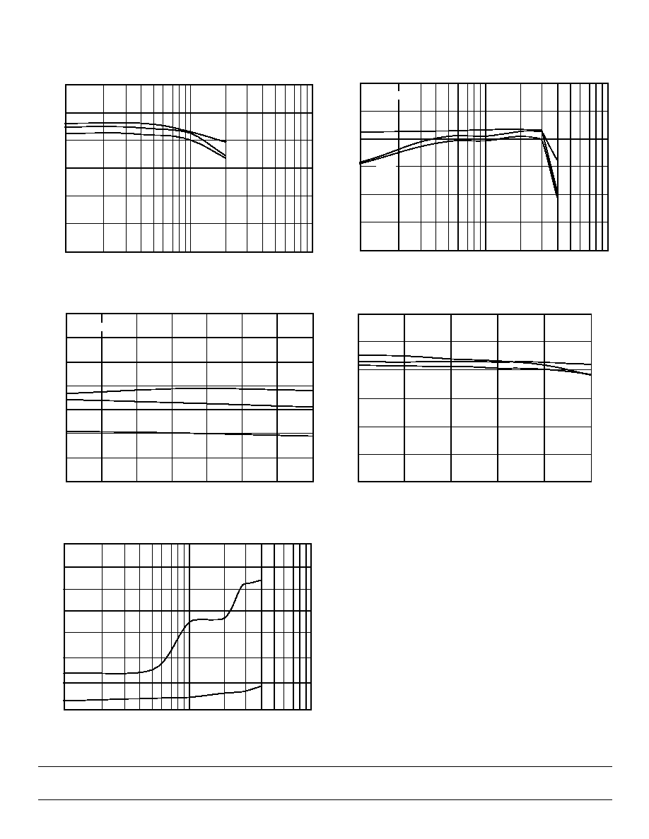
TYPICAL PERFORMANCE CHARACTERISTICS
THD
SNR
SINAD
THD, SNR, SINAD vs Input Frequency
Input Frequency (MHz)
THD
, SNR, SINAD (dB)
20
30
40
50
60
70
80
100
101
102
THD, SNR, SINAD vs Temperature
70
Temperature (∞C)
THD
, SNR, SINAD (dB)
56
58
60
62
64
66
68
0
25
70
THD
SNR
SINAD
fIN = 10 MHz
Power Dissipation vs Sample Rate
(Internal Reference)
P
o
w
er Dissipation (mW)
10 0
101
102
Sample Rate (MSPS)
Note: Bias1 and Bias2 optimized for each sample rate.
0
50
100
150
200
300
350
250
Sleep Mode
SINAD
SNR
THD
THD
, SNR, SINAD (dB)
20
30
40
50
60
70
80
10 0
101
102
THD, SNR, SINAD vs Sample Rate
Sample Rate (MSPS)
Note: Bias1 and Bias2 currents optimized for each sample rate.
SINAD
SNR
THD
fIN = 10 MHz
THD
SNR
SINAD
45
46
47
48
49
50
51
52
53
54
55
THD, SNR, SINAD (dB)
20
30
40
50
60
70
80
THD, SNR, SINAD vs Clock Duty Cycle
Clock Duty Cycle
THD
SNR
SINAD
5
8 / 1 / 0 0
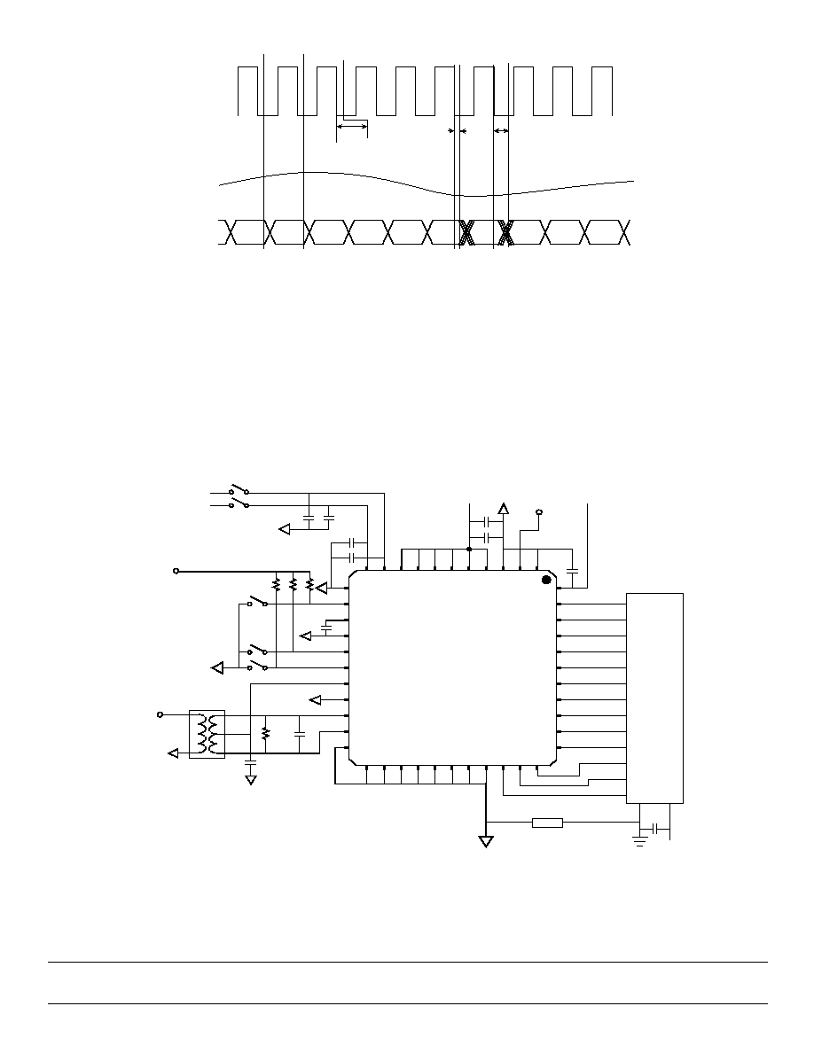
SPT7936
Data
N-1
Data
N
Data
N+1
Data
Analog Input
Clock
N+2
tH
S
A
M
P
L
E
tAP
S
A
M
P
L
E
N
S
A
M
P
L
E
N+1
tD
GENERAL DESCRIPTION
The SPT7936 is a low power, 12-bit, 28 MSPS ADC. It has a
pipelined architecture and incorporates digital error correc-
tion of the 11 most significant bits. This error correction
ensures good linearity performance for input frequencies up
to Nyquist. The inputs are fully differential, making the device
insensitive to system-level noise. This device can also be
used in a single-ended mode. (See analog input section.)
With the power dissipation roughly proportional to the sam-
pling rate, this device is ideal for very low power applications
in the range of 1 to 28 MSPS.
TYPICAL INTERFACE CIRCUIT
The SPT7936 requires few external components to achieve
the stated operation and performance. Figure 2 shows the
typical interface requirements when using the SPT7936 in
normal circuit operation. The following sections provide a descrip-
tion of the functions and outline critical performance criteria to
consider for achieving the optimal device performance.
Figure 1 - Timing Diagram
Figure 2 - Typical Interface Circuit
D8
D7
D6
D5
D4
D3
D2
D1
D0
VDD
2
D9
GND
GND
GND
GND
GND
GND
OR
GND
GND
D11
D10
VIN-
VIN+
GND
CM
Bias1
Bias0
GND
ExtRef
N/C
GND
Mini-Circuit
T1-6T
VIN
+3.3 V
+1.0 V
+2.0 V
1 k
1 k
1 k
+
+
4.7
µ
F
.01
µ
F
+
4.7
µ
F
.01
µ
F
+3.3 V
+3.3 V
.01
µ
F
(MSB)
(LSB)
Clock Input
(3.3 V Logic)
+3.3 V
FB
Bias1
Bias0
ExtRef
50
68 pF
.01
µ
F
SPT7936
(*)
V
DD
1
V
DD
1
V
DD
1
V
DD2
V
DD
2
V
DD
2
GND
V
REF
-
V
REF
+
CLK
GND
NOTES:
1) Place the ferrite bead (*) as close to the device as possible.
2) Place 0.01 microfarad capacitors as close to the device as possible.
3) All capacitors are surface-mount unless otherwise specified.
4) All input pins (references, analog input, clock input) must be
protected. (See absolute maximum rating.)
5) Set Bias1 and Bias0 for maximum sample rate.
Bias1Bias0
0
0
Sleep mode
0
1
Max. 5 MHz sampling
1
0
Max. 20 MHz sampling
1
1
Max. 28 MHz sampling
6) Use internal or external reference. Do not connect external voltage reference when using internal references.
7) All VDD1 and VDD2 must be connected together. Do not leave any pin unconnected.
8) All GND must be connected together. Do not leave any pin unconnected.
Interf
acing Logic
4.7
µ
F
.01
µ
F
.01
µ
F
BGAP