 | ÐлекÑÑоннÑй компоненÑ: SPT8100 | СкаÑаÑÑ:  PDF PDF  ZIP ZIP |
Äîêóìåíòàöèÿ è îïèñàíèÿ www.docs.chipfind.ru
SPT8100
16-BIT, 5 MSPS CMOS A/D CONVERTER
TECHNICAL DATA
JANUARY 9, 2002
FEATURES
· 16-bit, 5 MSPS CMOS analog-to-digital converter
· On-chip PGA: gain range from 0 to 19.5 dB in seven
selectable settings:
0 dB, +2.9 dB, +5.8 dB, +11.8 dB, +14.8 dB, +17.5 dB,
+19.5 dB
· DLE: ±0.5 LSB, ILE: ±1.25 LSB
· SFDR: 94 dB @
IN
= 900 kHz, 8.1 dBFS
· Internal sample-and-hold and voltage reference
· Power dissipation: 465 mW at 5 MSPS
· +5 V analog supply and +3.3 to +5.25 V digital output
supply
· 44-lead LQFP plastic package
APPLICATIONS
· Data acquisition systems
· IR imaging
· Scanners and digital copiers
· High-end CCD cameras
· Medical imaging
· Wireless communications
· Lab and test equipment
· Automatic test equipment
DESCRIPTION
The SPT8100 is a high-performance, 16-bit analog-to-
digital converter that operates at a sample rate of up to
5 MSPS. Excellent dynamic performance and high linear-
ity is achieved by a digitally calibrated pipelined architec-
ture fabricated in CMOS process technology.
A low-noise programmable gain amplifier (PGA) is also in-
corporated on chip. The PGA is digitally programmable in
seven selected settings over a 0 to +19.5 dB range. The
SPT8100 also features an on-chip internal sample-and-
hold and internal reference for minimal external circuitry.
It operates from a single +5 V supply. Total power dissipa-
tion, including internal reference, is 465 mW. A separate
digital output supply pin is provided for +3.3 V or 5 V logic
output levels. The SPT8100 is available in a 44-lead LQFP
package over the industrial temperature range of 40 °C to
+85 °C.
AGND
Low-Noise
PGA
16-bit, 5 MSPS ADC
VREF
GS2 GS0
(Gain Set)
V
IN
+
V
IN
16-bits
D15 D0
(Data Outputs)
OVR (Over-Range)
DV
DD
+5V
OV
DD
+3/5 V
BIAS
R
(Ext Bias
Resistor)
CLK
V
CM
OE (Output Enable)
BIAS
C
(Ext Bias
Capacitor)
RDY (Ready)
AV
DD
+5V
OGND
DGND
RS (Reset)
V
RT
V
RB
BLOCK DIAGRAM

2
1/9/02
SPT8100
ABSOLUTE MAXIMUM RATINGS (Beyond which damage may occur)
1
25 °C
Supply Voltages
AV
DD
...................................................................... +6 V
DV
DD
..................................................................... +6 V
OV
DD
..................................................................... +6 V
Input Voltages
Analog Input ................................. 0.5 V to V
DD
+0.5 V
CLK Input ............................................................... V
DD
AV
DD
DV
DD
.................................................. ±100 mV
Delta between AGND, DGND, and OGND ...... ±100 mV
Output
Digital Outputs .................................................... 10 mA
Temperature
Operating Temperature ........................... 40 to +85 °C
Junction Temperature ...................................... +175 °C
Lead Temperature (soldering 10 seconds) ...... +300 °C
Storage Temperature ............................ 65 to +150 °C
Note 1: Operation at any Absolute Maximum Rating is not implied. See
Electrical Specifications for proper nominal applied conditions in
typical applications.
ELECTRICAL SPECIFICATIONS
T
A
=T
MIN
to T
MAX
, AV
DD
=DV
DD
=+5.0 V, OV
DD
= 3.3 V,
S
=5 MSPS, 2.5 V
PP
input span, Gain=0 dB, R
EXT
=1.43 k
, unless
otherwise specified.
TEST
TEST
SPT8100
PARAMETERS
CONDITIONS
LEVEL
MIN
TYP
MAX
UNITS
Resolution
15.9
16
Bits
DC Accuracy
Integral Linearity Error (ILE)
V
±1.25
LSB
Differential Linearity Error (DLE)
V
±0.5
LSB
Gain Error
1
IV
7.5
+7.5
%FSR
Offset Error
2
IV
5
+5
%FSR
Analog Input (into PGA)
Differential Input Voltage Range
V
IN
+, V
IN
V
5
V
PPD
Input Capacitance
IV
15
pF
Input Resistance
3
PGA Gain = 0 dB
IV
5.5
k
Input Bandwidth
4
PGA Gain = 0 dB
V
12
MHz
Input Common Mode Voltage Range
V
1.15
2.40
3.65
V
Programmable Gain Amp
Composite Input-Referred
IN
> 300 kHz
Noise Floor
PGA Gain = 0 dB
V
1.4
LSB
RMS
PGA Gain = 2.9 dB
V
1.5
LSB
RMS
PGA Gain = 5.8 dB
V
1.6
LSB
RMS
PGA Gain = 11.8 dB
V
2.0
LSB
RMS
PGA Gain = 14.8 dB
V
2.3
LSB
RMS
PGA Gain = 17.5 dB
V
2.6
LSB
RMS
PGA Gain = 19.5 dB
V
2.8
LSB
RMS
PGA Range
V
19.5
dB
PGA Gain Steps
3
VI
0,2.9,5.8,11.8,14.8,17.5,19.5
dB
PGA Gain Accuracy
VI
±0.3
dB
Conversion Characteristics
Maximum Conversion Rate
VI
5
MSPS
Pipeline Delay (Latency)
5
IV
5.5
Clocks
Reset Pulse Time (
RS
)
IV
3
Clocks
Reset Calibration Time
FS = 5 MSPS
V
150
ms
References and External Bias
V
RT
V
RB
(Internal Ref)
VI
2.375
2.5
2.625
V
Bias Resistor Range (External)
V
800
1430
2500
V
CM
Output Voltage
IV
2.275
2.40
2.525
V
V
CM
Output Current
IV
47
µA
V
RT
V
3.45
3.65
3.85
V
V
RB
V
0.95
1.15
1.35
V
1
Total gain error of PGA and ADC using internal references.
2
Total offset error of PGA and ADC relative to mid-scale.
3
See table I for input resistance as a function of PGA gain.
4
Input bandwidth is a frequency to which the fundamental energy drops by 3 dB
5
The input is sampled on the falling edge of the clock and is available on the
output after the rising edge of the clock, 5.5 clock cycles later.
3
1/9/02
SPT8100
ELECTRICAL SPECIFICATIONS
T
A
=T
MIN
to T
MAX
, AV
DD
=DV
DD
=+5.0 V, OV
DD
= 3.3 V,
S
=5 MSPS, 2.5 V
PP
input span, Gain=0 dB, R
EXT
=1.43 k
, unless
otherwise specified.
TEST
TEST
SPT8100
PARAMETERS
CONDITIONS
LEVEL
MIN
TYP
MAX
UNITS
Dynamic Performance
1
Effective Number of Bits
ADC Input = 1 dBFS
2
IN
= 60 kHz
IV
12.2
13.0
Bits
IN
= 900 kHz
V
12.7
Bits
Signal-to-Noise Ratio
(without Harmonics)
ADC Input = 1 dBFS
2
IN
= 75 kHz
IV
78
81
dB
IN
= 900 kHz
V
80
dB
Harmonic Distortion
ADC Input = 0.5 dBFS
IN
= 60 kHz
IV
92
84
dB
IN
= 900 kHz
V
82
dB
Signal-to-Noise and Distortion
(SINAD)
ADC Input = 1 dBFS
IN
= 60 kHz
IV
75
80
dB
IN
= 900 kHz
V
78
dB
Spurious Free Dynamic Range
3
IN
= 60 kHz
ADC Input = 0.5 dB
IV
85
94
dBc
IN
= 900 kHz
V
94
dBc
IN
= 2 MHz
R
EXT
= 1 k
@ 10 MSPS
V
83
dBc
IN
= 3 MHz
R
EXT
= 1 k
@ 10 MSPS
V
78
dBc
Two-Tone Intermodulation
3rd Order Distortion
1
=400 kHz,
2
=410 kHz
4
V
94
dB
1
=890 kHz,
2
=900 kHz
5
V
89
dB
Inputs
GS0GS2 Logic 1 Voltage
VI
2.4
V
GS0GS2 Logic 0 Voltage
VI
0.8
V
CLK,
RS
Logic 1 Voltage
VI
2.0
V
CLK,
RS
Logic 0 Voltage
VI
0.8
V
Maximum Input Current Low
VI
10
+10
µA
Maximum Input Current High
VI
10
+10
µA
Input Capacitance
V
5
pF
Digital Outputs
Logic 1 Voltage
I
OH
= 2 mA
VI
OV
DD
0.5
V
Logic 0 Voltage
I
OL
= 2 mA
VI
0.4
V
CLK to Output Delay Time (t
D
)
C
LOAD
= 20 pF
IV
30
ns
Power Supply Requirements
Voltages
OV
DD
IV
3.0
3.3
5.25
V
AV
DD
IV
4.75
5.0
5.25
V
DV
DD
IV
4.75
5.0
5.25
V
Currents
I
DD
VI
93
103
mA
Power Dissipation
VI
465
515
mW
1
Dynamic performance tested at
S
=4.4 MSPS
2
0 dBFS is 5.0 V peak-to-peak differential
3
ADC Input = 8.1 dBFS, unless otherwise noted
4
Test Conditions: PGA setting of 5.8 dB; Analog Input at ADC = 0.7 dB
5
Test Conditions: PGA setting of 0 dB; Analog Input at ADC = 1.9 dB
TEST LEVEL CODES
All electrical characteristics are subject
to the following conditions:
All parameters having min/max specifi-
cations are guaranteed. The Test Level
column indicates the specific device
testing actually performed during
production and Quality Assurance
inspection. Any blank section in the data
column indicates that the specification is
not tested at the specified condition.
TEST LEVEL
TEST PROCEDURE
I
100% production tested at the specified temperature.
II
100% production tested at T
A
= +25 °C, and sample tested at the
specified temperatures.
III
QA sample tested only at the specified temperatures.
IV
Parameter is guaranteed (but not tested) by design and characteriza-
tion data.
V
Parameter is a typical value for information purposes only.
VI
100% production tested at T
A
= +25 °C. Parameter is guaranteed
over specified temperature range.
4
1/9/02
SPT8100
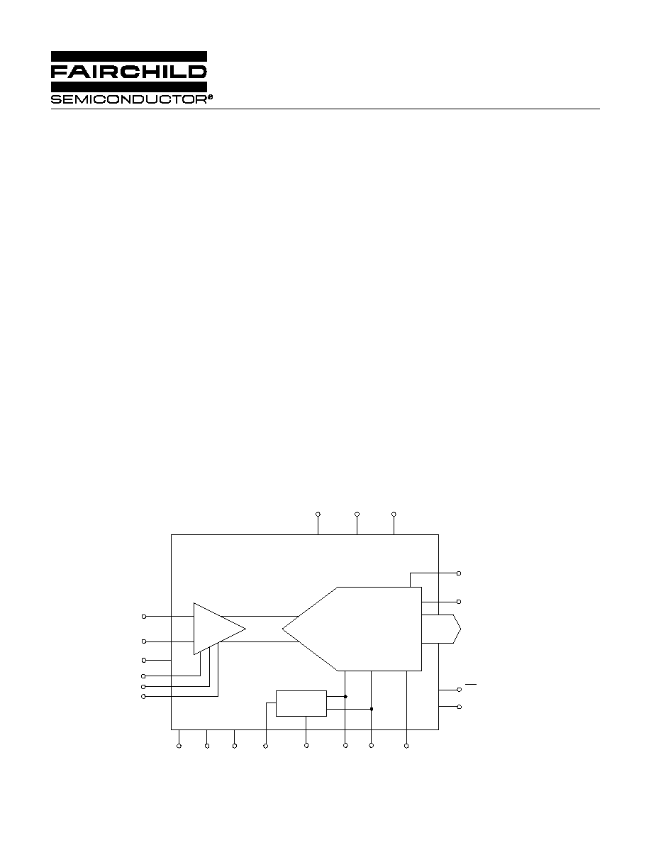
DEVICE OVERVIEW
The SPT8100 combines a high-resolution 5 MSPS 16-bit
ADC, a built-in reference, and a programmable gain amp-
lifier (PGA) with resistive input impedance in a 44-pin
package.
The device includes a digitally calibrated pipeline ADC,
which is calibrated on assertion of a simple reset signal.
The combination of low noise, high linearity, a high-input
impedance buffer (with programmable gain), wideband
S/H, on-board voltage references, and simple digital inter-
face (16-bit parallel output word synchronous with the
master sampling clock) makes the SPT8100 extremely
easy to use in a wide variety of systems.
For optimum performance, the analog inputs should be
driven differentially, and may be AC-coupled or DC-
coupled to a source. Typical applications include high-per-
formance data acquisition systems, automatic test equip-
ment, and wideband digital communications receivers
such as wireless basestations.
OPERATIONAL DESCRIPTION
The following sections describe in greater detail individual
blocks and functions of the SPT8100.
The incoming analog differential signal (maximum level 5 V
peak-to-peak differential) enters the device at the pins
V
IN
+/V
IN
. The analog signal path is partitioned into a pro-
grammable gain amplifier (PGA) and an ADC. The PGA
has maximum gain of +19.5 dB; the gain is set by the digi-
tal control signals GS0 to GS2.
The output of the PGA is fed directly to the ADC, which
samples at a rate equal to the CLK frequency and outputs
a 16-bit wide parallel word. The ADC uses a pipeline multi-
stage architecture. Latency is 5.5 clock cycles.
ADC CLOCK
The chip requires a single low-jitter clock to be applied at
the CLK pin, with nominal 4060% duty cycle. All clock
generation is performed internally and all converter and
S/H clocks in the ADC path are directly derived from CLK.
If the sample rate is changed by more than a factor of 2,
the device must be recalibrated using the
RS
(reset) pin.
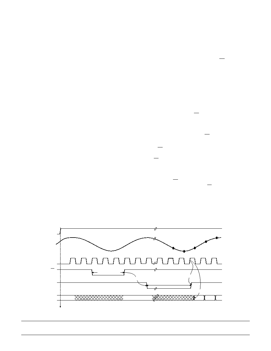
DEVICE STARTUP/INITIALIZATION SEQUENCE
Note: This initialization sequence is
required. Without
it, the device will not work.
Allow sufficient time for the analog blocks on the SPT8100
to power on and come up to their quiescent DC states.
Allowance may also be needed for thermal time constants
associated with the package/board.
On powerup, the SPT8100's
RS
(reset) should be held low
for at least three clock cycles. The power supply voltages
applied to the device must be stable during this time. The
clock signal (CLK) must be running for at least three clock
cycles prior to the rising edge of
RS
, and must continue
running.
When the
RS
signal goes from low to high, calibration is ini-
tiated. RDY is driven low two clock cycles after the rising
edge of
RS
, and will stay low for 150 ms with a 5 MHz clock.
When the initialization is complete, RDY returns high and
the device is ready for normal operation. Note that the cali-
bration of the ADC can be interrupted (before completion)
by changing the
RS
signal from high to low, which will
cause another reset to occur. When
RS
goes from low back
to high, another calibration cycle will begin.
RDY cannot be tri-stated: it is always driven either high or
low. The CLK must be constantly running throughout the
Figure 1 Device Initialization Timing
Requires external reset on powerup
3 clock cycles min
Initialization period: 150 ms with 5 MHz clock
N
N+1
N+2
INVALID DATA
N+5
N+6
N+7
24 ns typ
N+8
PWR ON
A
IN
CLK
RS
RDY
D
OUT
N+4
2 clock cycles
5 ns typ

5
1/9/02
SPT8100
initialization phase until RDY is deasserted. Note that,
although typically the device is initialized when power is
first applied, the initialization is only started when the
RS
is
asserted; there is no "power-on-reset" circuitry on chip.
RS
may be held low for an indefinite period of time. While
RS
is
low, RDY will remain high. After
RS
is returned to high, RDY
will go low for the duration of the calibration.
PROGRAMMABLE GAIN AMPLIFIER
The programmable gain amplifier (PGA) precedes the
ADC inputs. The differential inputs, which are resistive, are
at pins V
IN
+ and V
IN
.The maximum input range is 5 V
peak-to-peak differential (2.5 V single-ended). To achieve
maximum overall system noise performance, the source
driving these inputs needs to be as low-noise and as low-
jitter as possible, while maintaining the required distortion
performance. In addition, the driving source must be low
impedance to maintain the accuracy of the PGA gain.
The internal 0 dB analog signal level and ADC full-scale
output level is 5 V peak-to-peak differential (2.5 V single-
ended). The PGA may be used to provide gain for an input
less than 5 V peak-to-peak differential.
The gain of the PGA can be programmed using a three-bit
control, available at pins GS0 to GS2. See table I. Note that
the input resistance is a function of the gain setting.
Table I PGA Gain Control
PGA
Input
V/V
3 dB
GS2 GS1 GS0
Gain Resistance Gain
BW
LSB
RMS
(dB)
(k
)
0
0
0
0
5.57
1
12
1.4
0
0
1
2.9
4.65
1.40
10
1.5
0
1
0
5.8
3.97
1.95
8
1.6
0
1
1
11.8
2.23
3.9
7
2.0
1
0
0
14.8
1.66
5.5
6
2.3
1
0
1
17.5
1.25
7.5
5.5
2.6
1
1
0
19.5
1.00
9.5
5
2.8
1
1
1
X
Forbidden
TYPICAL INTERFACE CIRCUIT
ANALOG INPUT DRIVER
The differential analog inputs (V
IN
+, V
IN
) have a resistive
input impedance of 1 k
minimum. For best performance,
the input source should be a differential input, as shown in
figure 2, typical interface circuit. The SPT8100 provides its
own common-mode voltage on the pin marked V
CM
. Out-
put drive capability of V
CM
is a maximum of 47 µA (50 k
to
ground).
The SPT8100 application note (AN8100) shows an ex-
ample of two modes of driving the SPT8100. One mode is
through a transformer and the other is through a single-to-
differential converter. In all cases, both inputs V
IN
+ and
V
IN
must be kept within the input common-mode range
(1.15 V to 3.65 V).
BIAS
C
CONNECTION
An external capacitor, C
EXT
on the BIAS
C
pin, is used only
for noise filtering of an internal voltage associated with the
references. Its value is not critical: 1 µF in parallel with
0.01 µF is recommended.
BIAS
R
CONNECTION
As shown in the typical interface circuit, R
EXT
is needed to
connect between BIAS
R
to ground. This resistor ranges
from 800
to 2.5 k
. The proper selection of R
EXT
is a
function of the sample rate and input frequency. Nominally,
at 5 MSPS, R
EXT
=1.43 k
is recommended. If linearity for
large signal levels at an analog bandwidth of 2 MHz is criti-
cal, the value should be decreased to R
EXT
=1.24 k
; and
for even higher-frequency analog inputs, R
EXT
=1.0 k
can
be used. At lower sample rates (for example 2 MSPS),
and lower analog input frequencies, the value may be in-
creased to R
EXT
=2 k
. (Refer to the typical interface circuit
table in figure 2b.)
POWER SUPPLIES AND GROUNDING
The SPT8100 requires three power supplies: analog AV
DD
,
digital DV
DD
and output supply OV
DD
. This device works
best if all three supplies are coming from the analog supply
side of the system as shown in the typical interface circuit
(figure 2a).
Note, in figure 2a, that the supplies to the logic interface
circuit and the OV
DD
are separate from each other. In a
case where the +A3.3/5 V supply is not available, try to
implement the design as close as possible to that shown
in figure 2b. Place the ferrite bead (FB1) as close to the
device as possible. To avoid latch-up, the delta between
all three grounds must stay with 100 mV; this includes
transients. (Refer to the absolute maximum ratings
specifications.)