SPT9713
12-BIT, 100 MWPS TTL D/A CONVERTER
TECHNICAL DATA
FEBRUARY 15, 2001
APPLICATIONS
∑ Fast frequency hopping spread spectrum radios
∑ Direct sequence spread spectrum radios
∑ Microwave and satellite modems
∑ Test & measurement instrumentation
FEATURES
∑ 12-Bit, 100 MWPS digital-to-analog converter
∑ TTL compatibility
∑ Low power: 640 mW
∑ 1/2 LSB DNL
∑ 40 MHz multiplying bandwidth
∑ Industrial temperature range
∑ Superior performance over AD9713
≠ Improved settling time of 13 ns
≠ Improved glitch energy 15 pV-s
≠ Master-slave latches
GENERAL DESCRIPTION
The SPT9713 is a 12-bit, 100 MWPS digital-to-analog
converter designed for direct digital synthesis, high reso-
lution imaging, and arbitrary waveform generation applica-
tions.
This device is pin-for-pin compatible with the AD9713 with
significantly improved performance. The only difference
between the SPT9713 and the AD9713 is that the Latch
Enable (LE, pin 26) for the SPT9713 is rising-edge trig-
gered (see figure 1), whereas the Latch Enable (LE, pin
26) for the AD9713 functions in the transparent mode.
The SPT9713 is a TTL-compatible device. It features a
fast settling time of 13 ns and low glitch impulse energy of
15 pV-s, which results in excellent spurious-free dynamic
range characteristics.
The SPT9713 is available in a 28-lead PLCC package in
the industrial temperature range (≠40 to +85 ∞C).
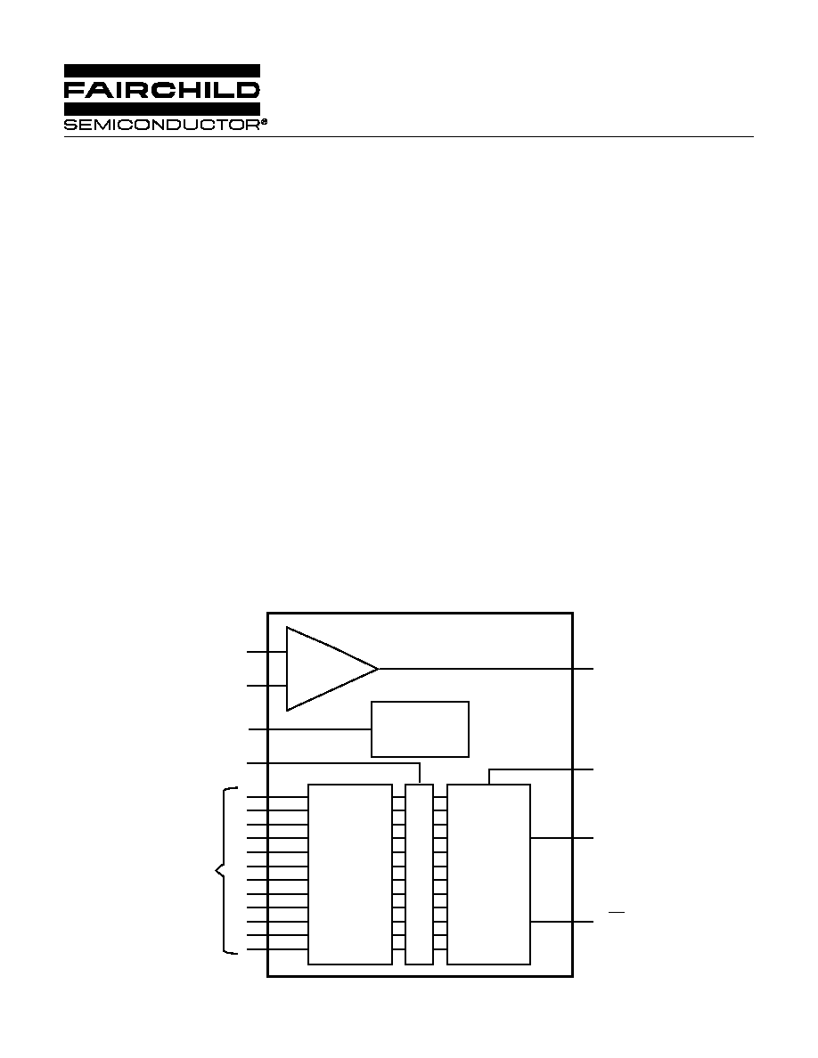
BLOCK DIAGRAM
(MSB)
Latch Enable
Digital
Inputs
D1
through
D12
Ref In
I
Out
I
Out
Decoders
and
Drivers
Latches
(LSB)
R
Set
Control Amp In
Control
Amp Out
Internal
Voltage
Reference
Ref Out
Switch
Network
Control
Amp
+

2
2/15/01
SPT9713
ABSOLUTE MAXIMUM RATINGS (Beyond which damage may occur)
1
25 ∞C
Note: 1. Operation at any Absolute Maximum Rating is not implied. See
Electrical Specifications for proper nominal applied conditions
in typical applications.
Supply Voltages
Positive Supply Voltage (V
CC
) ................................ +7 V
Negative Supply Voltage (V
EE
) .............................. ≠7 V
A/D Ground Voltage Differential ........................... 0.5 V
Input Voltages
Digital Input Voltage
(D1≠D12, Latch Enable) ............................... 0 V to V
CC
Control Amp Input Voltage Range ............... 0 V to ≠4 V
Reference Input Voltage Range (V
REF
) ........ 0 V to V
EE
Output Currents
Internal Reference Output Current .................... 500 µA
Control Amplifier Output Current ..................... ±2.5 mA
Temperature
Operating Temperature .......................... ≠40 to +85 ∞C
Junction Temperature ...................................... +150 ∞C
Lead, Soldering (10 seconds) ......................... +300 ∞C
Storage ................................................ ≠65 to +150 ∞C
ELECTRICAL SPECIFICATIONS
T
A
= T
MIN
≠ T
MAX
, V
CC
= +5.0 V, V
EE
= ≠5.2 V, R
Set
= 7.5 k
, Control Amp In = Ref Out, V
OUT
= 0 V, unless otherwise specified.
TEST
TEST
SPT9713A
SPT9713B
PARAMETERS
CONDITIONS
LEVEL
MIN
TYP
MAX
MIN
TYP
MAX
UNITS
DC Performance
Resolution
12
12
Bits
Differential Linearity
I
±0.5
±0.75
±1.0
±1.25
LSB
Differential Linearity
Max at Full Temp.
VI
±1.5
±2.0
LSB
Integral Linearity
Best Fit
I
±0.75
±1.0
±1.0
±1.5
LSB
Integral Linearity
Max at Full Temp.
VI
±1.75
±2.0
LSB
Output Capacitance
+25 ∞C
V
10
10
pF
Gain Error
1
+25 ∞C
I
1.0
5.0
1.0
5.0
% FS
Full Temp.
VI
8.0
8.0
% FS
Gain Error Tempco
Full Temp.
V
150
150
PPM/∞C
Zero-Scale Offset Error
+25 ∞C
I
0.5
2.5
0.5
2.5
µA
Full Temp.
VI
5.0
5.0
µA
Offset Drift Coefficient
Full Temp.
V
0.01
0.01
µA/∞C
Output Compliance Voltage
+25 ∞C
IV
≠1.2
+2.0
≠1.2
+2.0
V
Equivalent Output Resistance
+25 ∞C
IV
0.8
1.0
1.2
0.8
1.0
1.2
k
Dynamic Performance
Conversion Rate
+25 ∞C
IV
100
100
MWPS
Settling Time t
ST2
+25 ∞C
V
13
13
ns
Output Propagation Delay t
D3
+25 ∞C
V
2
2
ns
Glitch Energy
4
+25 ∞C
V
15
15
pV-s
Full Scale Output Current
5
+25 ∞C
V
20.48
20.48
mA
Spurious-Free Dynamic Range
6
+25 ∞C
1.23 MHz; 10 MWPS
2 MHz Span
V
70
70
dBc
5.055 MHz; 20 MWPS
2 MHz Span
V
68
68
dBc
10.1 MHz; 50 MWPS
2 MHz Span
V
68
68
dBc
16 MHz; 40 MWPS
10 MHz Span
V
68
68
dBc
Rise Time / Fall Time
R
L
= 50
V
2
2
ns
1
Gain is measured as a ratio of the full-scale current to I
Set
. The ratio is nominally 128.
2
Measured as voltage at mid-scale transition to ±0.024%; R
L
=50
.
3
Measured from the rising edge of Latch Enable to where the output signal has left a 1 LSB error band.
4
Glitch is measured as the largest single transient.
5
Calculated using I
FS
= 128 x (Control Amp In / R
Set
)
6
SFDR is defined as the difference in signal energy between the fundamental and worst case spurious frequencies in the output spectrum window,
which is centered at the fundamental frequency and covers the indicated span.

3
2/15/01
SPT9713
TEST LEVEL CODES
All electrical characteristics are subject to the
following conditions:
All parameters having min/max specifications
are guaranteed. The Test Level column indi-
cates the specific device testing actually per-
formed during production and Quality Assur-
ance inspection. Any blank section in the data
column indicates that the specification is not
tested at the specified condition.
LEVEL
TEST PROCEDURE
I
100% production tested at the specified temperature.
II
100% production tested at T
A
= +25 ∞C, and sample tested at the
specified temperatures.
III
QA sample tested only at the specified temperatures.
IV
Parameter is guaranteed (but not tested) by design and characteri-
zation data.
V
Parameter is a typical value for information purposes only.
VI
100% production tested at T
A
= +25 ∞C. Parameter is guaranteed
over specified temperature range.
ELECTRICAL SPECIFICATIONS
T
A
= T
MIN
≠ T
MAX
, V
CC
= +5.0 V, V
EE
= ≠5.2 V, R
SET
= 7.5 k
, Control Amp In = Ref Out, V
OUT
= 0 V, unless otherwise specified.
TEST
TEST
SPT9713A
SPT9713B
PARAMETERS
CONDITIONS
LEVEL
MIN
TYP
MAX
MIN
TYP
MAX
UNITS
Power Supply Requirements
Positive Supply Voltage
IV
4.75
5.0
+5.25
4.75
5.0
+5.25
V
Negative Supply Voltage
IV
≠5.46
≠5.2
≠4.94
≠5.46
≠5.2
≠4.94
V
Positive Supply Current (+5.0 V)
+25 ∞C
I
8
14
8
14
mA
Full Temp.
VI
16
16
mA
Negative Supply Current (≠5.2 V)
+25 ∞C
I
115
140
115
140
mA
Full Temp
VI
148
148
mA
Nominal Power Dissipation
V
640
640
mW
Power Supply Rejection Ratio
±5% of V
EE
and V
CC
I
30
100
30
100
µA/V
External Ref, +25 ∞C
Voltage Input and Control
Reference Input Impedance
+25 ∞C
V
3
3
k
Ref. Multiplying Bandwidth
+25 ∞C
V
40
40
MHz
Internal Reference Voltage
VI
≠1.15 ≠1.20 ≠1.25
≠1.15 ≠1.20 ≠1.25
V
Internal Reference Voltage Drift
Full
V
50
50
ppm/∞C
Amplifier Input Impedance
+25 ∞C
V
3
3
M
Amplifier Input Bandwidth
+25 ∞C
V
1
1
MHz
Digital Inputs
Logic 1 Voltage
Full Temp.
VI
2.0
2.0
V
Logic 0 Voltage
Full Temp.
VI
0.8
0.8
V
Logic 1 Current
Full Temp.
VI
20
20
µA
Logic 0 Current
Full Temp.
VI
600
600
µA
Input Capacitance
+25 ∞C
V
3
3
pF
Input Setup Time ≠ t
S
+25 ∞C
IV
3
2
3
2
ns
Input Setup Time ≠ t
S
Full Temp.
IV
3.5
3.5
ns
Input Hold Time ≠ t
H
+25 ∞C
IV
0.5
0
0.5
0
ns
Input Hold Time ≠ t
H
Full Temp.
IV
0.5
0.5
ns
Latch Pulse Width ≠
t
PWL
,
t
PWH
+25 ∞C
IV
5.0
4.0
5.0
4.0
ns

4
2/15/01
SPT9713
THEORY OF OPERATION
The SPT9713 uses a segmented architecture incorporat-
ing most significant bit (MSB) decoding. The four MSBs
(D1≠D4) are decoded to thermometer code lines to drive
15 discrete current sinks. For the eight least significant
bits (LSBs), D5 and D6 are binary weighted and D7≠D12
are applied to the R-2R network. The 12-bit decoded data
is input to internal master/slave latches. The latched data
is input to the switching network and is presented on the
output pins as complementary current outputs.
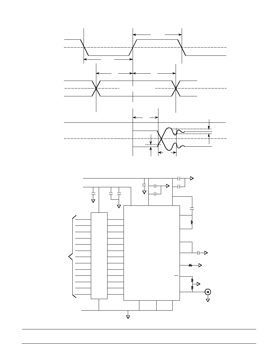
TYPICAL INTERFACE CIRCUIT
The SPT9713 requires few external components to
achieve the stated operation and performance. Figure 2
shows the typical interface requirements when using the
SPT9713 in normal circuit operation. The following sec-
tions provide descriptions of the pin functions and outline
critical performance criteria to consider for achieving opti-
mal device performance.
POWER SUPPLIES AND GROUNDING
The SPT9713 requires the use of +5 V and ≠5.2 V sup-
plies. All supplies should be treated as analog supply
sources. This means the ground returns of the device
should be connected to the analog ground plane. All sup-
ply pins should be bypassed with .01 µF and 10 µF
decoupling capacitors as close to the device as possible.
The two grounds available on the SPT9713 are DGND
and AGND. These grounds are not tied together internal to
the device. The use of ground planes is recommended to
achieve the best performance of the SPT9713. All ground,
reference and analog output pins should be tied directly to
the DAC ground plane. The DAC and system ground
planes should be separate from each other and only con-
nected at a single point through a ferrite bead to reduce
ground noise pickup.
DIGITAL INPUTS AND TIMING
The SPT9713 uses TTL logic drivers for each data input
D1≠D12 and Latch Enable. It also employs master/slave
latches to simplify digital interface timing requirements
and reduce glitch energy by synchronizing the current
switches. This is an improvement over the AD9713, which
typically requires external latches for digital input synchro-
nization.
Referring to figure 1, data is latched into the DAC on the
rising edge of the latch enable clock with the associated
setup and hold times. The output transition occurs after a
typical 2 ns propagation delay and settles to within ±1 LSB
in typically 13 ns. Because of the SPT9713's rising-edge
triggering, no timing changes are required when replacing
an AD9713 operating in the transparent mode.
VOLTAGE REFERENCE
When using the internal reference, Ref Out should be con-
nected to Control Amp In and decoupled with a 0.1 µF
capacitor. Control Amp Out should be connected to Ref In
and decoupled to the analog supply. (See figure 2.)
Full-scale output current is determined by Control Amp In
and R
Set
using the following formula:
I
Out
(FS) = (Control Amp In / R
Set
) x 128
(Current Out is a constant 128 factor of the
reference current)
The internal reference is typically ≠1.20 V with a tolerance
of ±0.05 V and a typical drift of 50 ppm/∞C. If greater accu-
racy or temperature stability is required, an external refer-
ence can be utilized.
OUTPUTS
The output of the SPT9713 is comprised of complemen-
tary current sinks, I
Out
and I
Out
. The output current levels
at either I
Out
or I
Out
are based upon the digital input code.
The sum of the two is always equal to the full-scale output
current minus one LSB.
By terminating the output current through a resistive load
to ground, an associated voltage develops. The effective
resistive load (R
Eff
) is the output resistance of the device
(R
Out
) in parallel with the resistive load (R
L
). The voltage
which develops can be determined using the following
formulas:
Control Amp Out = ≠1.2 V, and R
Set
= 7.5 k
I
Out
(FS) = (≠1.2 V / 7.5 k
) x 128 = ≠20.48 mA
R
L
= 51
R
Out
= 1.0 k
R
Eff
= 51
|| 1.0 k
= 48.52
V
Out
= R
Eff
x I
Out
(FS) = 48.52
x ≠20.48 mA
= ≠0.994 V
The resistive load of the SPT9713 can be modified to in-
corporate a wide variety of signal levels. However, optimal
device performance is achieved when the outputs are
equivalently loaded.
5
2/15/01
SPT9713
Figure 1 ≠ Timing Diagram
Latch
Enable
t
PWL
t
H
t
S
t
PWH
OUT+
OUT
1/2 LSB
t
ST
1 LSB
t
D
Data Inputs
15,25
12,21
0.1 µF
0.1 µF
0.001 µF
0.001 µF
+5 V
23
0.1 µF
0.01 µF
AV
EE
R
L
R
L
14
16
I
Out
I
Out
R
Set
24
R
Set
19
20
Control
Amp In
Ref Out
Control
Amp Out
18
17
20 W
Ref In
D1 (MSB)
D2
D3
D4
D5
D6
D7
D8
D9
D10
D11
D12 (LSB)
LE
28
1
2
3
4
5
6
7
8
9
10
11
26
DGND AGND Ref GND
System
GND
TTL Logic Drivers
0.1 µF
5.2 V
V
Out
Digital Inputs
Clock
Input
SPT9713
27 13 22
DV
EE
DV
CC
10 µF
10 µF
0.1 µF
Figure 2 ≠ Typical Interface Circuit
6
2/15/01
SPT9713
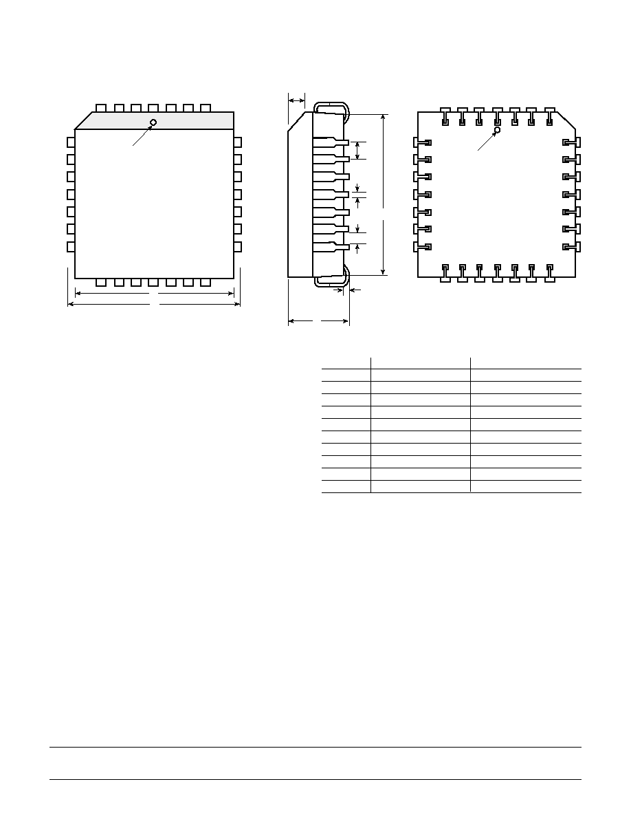
PACKAGE OUTLINE
28-Lead PLCC
A
B
Pin 1
C
D
E
F
G
H
TOP
VIEW
Pin 1
BOTTOM
VIEW
I
INCHES
MILLIMETERS
SYMBOL
MIN
MAX
MIN
MAX
A
0.452
0.456
11.48
11.58
B
0.485
0.495
12.32
12.57
C
30∞
30∞
D
0.170
0.179
4.32
4.55
E
0.020
0.025
0.51
0.64
F
0.031
0.035
0.79
0.89
G
0.013
0.021
0.33
0.53
H
0.048
0.052
1.22
1.32
I
0.410
0.430
10.41
10.92
7
2/15/01
SPT9713
ORDERING INFORMATION
PART NUMBER
DNL/INL
TEMPERATURE RANGE
PACKAGE
SPT9713AIP
±0.75/±1.0
≠40 to +85 ∞C
28L PLCC
SPT9713BIP
±1.25/±1.5
≠40 to +85 ∞C
28L PLCC
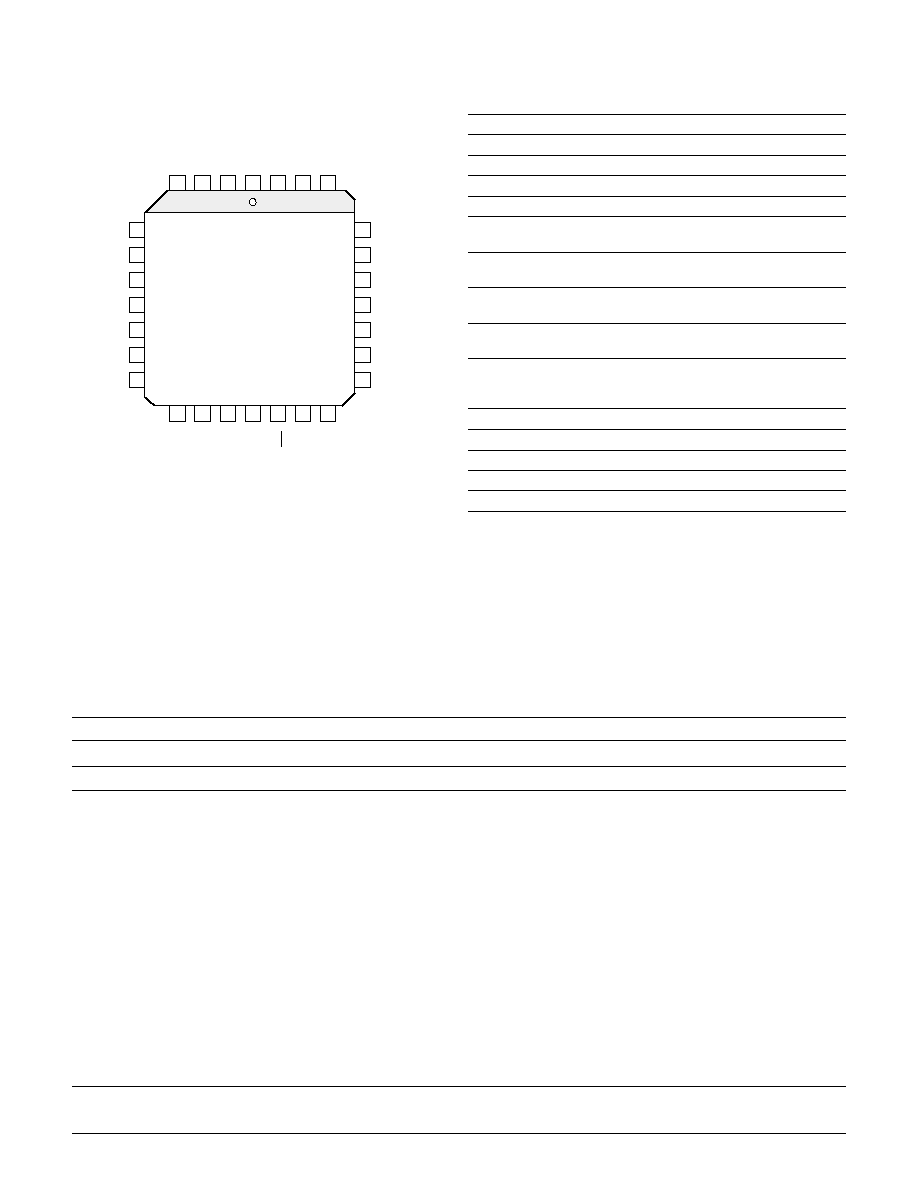
PIN ASSIGNMENTS
PIN FUNCTIONS
Name
Function
Out+
Analog Current Output
Out≠
Complementary Analog Current Output
D1≠D12
Digital Input Bits (D12 is the LSB)
Latch Enable
Latch Control Line
Ref In
Voltage Reference Input
Ref Out
Internal Voltage Reference Output
Normally Connected to Control Amp In
Ref GND
Ground Return For Internal Voltage
Reference and Amplifier
Control Amp In
Normally Connected to Ref Out If Not
Connected to External Reference
Control Amp Out Output of Internal Control Amplifier
Normally Connected to Ref In
R
Set1
Connection for External Resistance
Reference When Using Internal Amplifier
Nominally 7.5 k
Analog Return
Analog Return Ground
Analog V
EE
Analog Negative Supply (≠5.2 V)
Digital V
EE
Digital Negative Supply (≠5.2 V)
Digital V
CC
Digital Positive Supply (+5.2 V)
DGND
Digital Ground Return
1Full-Scale Current Out = 128 (Control Amp In / R
Set
)
25
24
23
22
21
20
19
5
6
7
8
9
10
11
18
17
16
15
14
13
12
26
27
28
1
2
3
4
Analog V
EE
R
Set
Digital V
CC
Ref GND
Digital V
EE
Ref Out
Control Amp In
D6
D7
D8
D9
D10
D11
(LSB) D12
Latch Enable
DGND
(MSB) D1
D2
D3
D4
D5
Control Amp Out
Ref In
Analog V
EE
I
Out
Analog Return
Digital V
EE
I
Out
PLCC
LIFE SUPPORT POLICY
FAIRCHILD'S PRODUCTS ARE NOT AUTHORIZED FOR USE AS CRITICAL COMPONENTS IN LIFE SUPPORT DEVICES OR SYSTEMS
WITHOUT THE EXPRESS WRITTEN APPROVAL OF THE PRESIDENT OF FAIRCHILD SEMICONDUCTOR CORPORATION. As used herein:
1. Life support devices or systems are devices or systems which, (a) are
intended for surgical implant into the body, or (b) support or sustain life,
and whose failure to perform, when properly used in accordance with
instructions for use provided in the labeling, can be reasonably
expected to result in a significant injury to the user.
2. A critical component is any component of a life support device or
system whose failure to perform can be reasonably expected to cause
the failure of the life support device or system, or to affect its safety or
effectiveness.
DISCLAIMER
FAIRCHILD SEMICONDUCTOR RESERVES THE RIGHT TO MAKE CHANGES WITHOUT FURTHER NOTICE TO ANY PRODUCTS HEREIN TO
IMPROVE RELIABILITY, FUNCTION OR DESIGN. FAIRCHILD DOES NOT ASSUME ANY LIABILITY ARISING OUT OF THE APPLICATION OR
USE OF ANY PRODUCT OR CIRCUIT DESCRIBED HEREIN; NEITHER DOES IT CONVEY ANY LICENSE UNDER ITS PATENT RIGHTS, NOR
THE RIGHTS OF OTHERS.
www.fairchildsemi.com
© Copyright 2002 Fairchild Semiconductor Corporation