 | ÐлекÑÑоннÑй компоненÑ: SSF17N60A | СкаÑаÑÑ:  PDF PDF  ZIP ZIP |
Äîêóìåíòàöèÿ è îïèñàíèÿ www.docs.chipfind.ru
Avalanche Rugged Technology
Rugged Gate Oxide Technology
Lower Input Capacitance
Improved Gate Charge
Extended Safe Operating Area
Lower Leakage Current : 25 A (Max.) @ V
DS
= 600V
Lower R
DS(ON)
: 0.356 (Typ.)
Advanced Power MOSFET
Thermal Resistance
Junction-to-Case
Junction-to-Ambient
R
JC
R
JA
Characteristic
Max.
Units
Symbol
Typ.
FEATURES
Absolute Maximum Ratings
Drain-to-Source Voltage
Continuous Drain Current (T
C
=25 )
Continuous Drain Current (T
C
=100 )
Drain Current-Pulsed
Gate-to-Source Voltage
Single Pulsed Avalanche Energy
Avalanche Current
Repetitive Avalanche Energy
Peak Diode Recovery dv/dt
Total Power Dissipation (T
C
=25 )
Linear Derating Factor
Operating Junction and
Storage Temperature Range
Maximum Lead Temp. for Soldering
Purposes, 1/8" from case for 5-seconds
Characteristic
Value
Units
Symbol
I
DM
V
GS
E
AS
I
AR
E
AR
dv/dt
I
D
P
D
T
J
, T
STG
T
L
A
V
mJ
A
mJ
V/ns
W
A
V
DSS
V
TO-3PF
1.Gate 2. Drain 3. Source
3
2
1
O
1
O
2
O
3
O
1
O
1
o
C
o
C
o
C
o
C
µ
W/
o
C
o
C/W
SSF17N60A
BV
DSS
= 600 V
R
DS(on)
= 0.45
I
D
= 9 A
600
9
5.7
68
884
9
10
3.0
100
0.8
- 55 to +150
300
1.25
40
--
--
30
+
_
©1999 Fairchild Semiconductor Corporation
Rev. B
N-CHANNEL
POWER MOSFET
Electrical Characteristics
(T
C
=25 unless otherwise specified)
Drain-Source Breakdown Voltage
Breakdown Voltage Temp. Coeff.
Gate Threshold Voltage
Gate-Source Leakage , Forward
Gate-Source Leakage , Reverse
Characteristic
Symbol
Max. Units
Typ.
Min.
Test Condition
Static Drain-Source
On-State Resistance
Forward Transconductance
Input Capacitance
Output Capacitance
Reverse Transfer Capacitance
Turn-On Delay Time
Rise Time
Turn-Off Delay Time
Fall Time
Total Gate Charge
Gate-Source Charge
Gate-Drain("Miller") Charge
g
fs
C
iss
C
oss
C
rss
t
d(on)
t
r
t
d(off)
t
f
Q
g
Q
gs
Q
gd
BV
DSS
BV/ T
J
V
GS(th)
R
DS(on)
I
GSS
I
DSS
V
V
nA
A
pF
ns
nC
--
--
--
--
--
--
--
--
--
--
--
--
--
V
GS
=0V,I
D
=250 A
I
D
=250 A See Fig 7
V
DS
=5V,I
D
=250 A
V
GS
=30V
V
GS
=-30V
V
DS
=600V
V
DS
=480V,T
C
=125
V
GS
=10V,I
D
=4.5A
V
DS
=50V,I
D
=4.5A
V
DD
=300V,I
D
=17A,
R
G
=5.3
See Fig 13
V
DS
=480V,V
GS
=10V,
I
D
=17A
See Fig 6 & Fig 12
Drain-to-Source Leakage Current
V
GS
=0V,V
DS
=25V,f =1MHz
See Fig 5
Source-Drain Diode Ratings and Characteristics
Continuous Source Current
Pulsed-Source Current
Diode Forward Voltage
Reverse Recovery Time
Reverse Recovery Charge
I
S
I
SM
V
SD
t
rr
Q
rr
Characteristic
Symbol
Max. Units
Typ.
Min.
Test Condition
--
--
--
--
--
A
V
ns
C
Integral reverse pn-diode
in the MOSFET
T
J
=25 ,I
S
=9A,V
GS
=0V
T
J
=25 ,I
F
=17A
di
F
/dt=100A/ s
o
C
V/
o
C
µ
µ
µ
µ
µ
O
1
O
4
O
4
o
C
o
C
O
4
O
4
O
5
O
4
O
4
O
5
o
C
µ
SSF17N60A
600
--
2.0
--
--
--
--
--
0.72
--
--
--
--
--
330
136
23
26
112
36
128
18
53.4
--
--
4.0
100
-100
25
250
0.45
--
3960
380
160
55
60
235
80
166
--
--
10.72
3050
--
--
--
570
8.5
9
68
1.4
--
--
Notes ;
Repetitive Rating : Pulse Width Limited by Maximum Junction Temperature
L=20mH, I
AS
=9A, V
DD
=50V, R
G
=27 , Starting T
J
=25
I
SD
17A, di/dt 200A/ s, V
DD
BV
DSS
, Starting T
J
=25
Pulse Test : Pulse Width = 250 s, Duty Cycle 2%
Essentially Independent of Operating Temperature
<
_
<
_
<
_
<
_
O
1
O
2
O
3
O
4
O
5
o
C
o
C
µ
µ
N-CHANNEL
POWER MOSFET
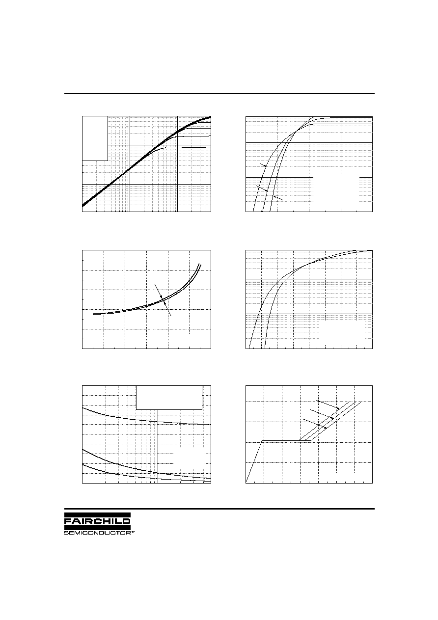
Fig 1. Output Characteristics
Fig 2. Transfer Characteristics
Fig 6. Gate Charge vs. Gate-Source Voltage
Fig 5. Capacitance vs. Drain-Source Voltage
Fig 4. Source-Drain Diode Forward Voltage
Fig 3. On-Resistance vs. Drain Current
SSH17N60A
10
-1
10
0
10
1
10
0
10
1
@ Notes :
1. 250
µ
s Pulse Test
2. T
C
= 25
o
C
V
GS
Top : 1 5 V
1 0 V
8.0 V
7.0 V
6.0 V
5.5 V
5.0 V
Bottom : 4.5 V
I
D
, Drain Current [A]
V
DS
, Drain-Source Voltage [V]
2
4
6
8
10
10
-1
10
0
10
1
25
o
C
150
o
C
- 55
o
C
@ Notes :
1. V
GS
= 0 V
2. V
DS
= 50 V
3. 250
µ
s Pulse Test
I
D
, Drain Current [A]
V
GS
, Gate-Source Voltage [V]
0
10
20
30
40
50
60
0.0
0.2
0.4
0.6
0.8
1.0
@ Note : T
J
= 25
o
C
V
GS
= 20 V
V
GS
= 10 V
R
DS(on)
, [
]
Drain-Source On-Resistance
I
D
, Drain Current [A]
0.4
0.6
0.8
1.0
1.2
1.4
1.6
1.8
2.0
10
-1
10
0
10
1
150
o
C
25
o
C
@ Notes :
1. V
GS
= 0 V
2. 250
µ
s Pulse Test
I
DR
, Reverse Drain Current [A]
V
SD
, Source-Drain Voltage [V]
10
0
10
1
0
1000
2000
3000
4000
5000
C
iss
= C
gs
+ C
gd
( C
ds
= shorted )
C
oss
= C
ds
+ C
gd
C
rss
= C
gd
@ Notes :
1. V
GS
= 0 V
2. f = 1 MHz
C
rss
C
oss
C
iss
Capacitance [pF]
V
DS
, Drain-Source Voltage [V]
0
20
40
60
80
100
120
140
0
5
10
V
DS
= 480 V
V
DS
= 300 V
V
DS
= 120 V
@ Notes : I
D
= 17.0 A
V
GS
, Gate-Source Voltage [V]
Q
G
, Total Gate Charge [nC]
N-CHANNEL
POWER MOSFET
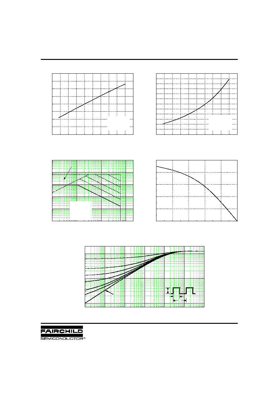
Fig 7. Breakdown Voltage vs. Temperature
Fig 8. On-Resistance vs. Temperature
Fig 11. Thermal Response
Fig 10. Max. Drain Current vs. Case Temperature
Fig 9. Max. Safe Operating Area
P
DM
t
1
t
2
SSF17N60A
-75
-50
-25
0
25
50
75
100
125
150
175
0.8
0.9
1.0
1.1
1.2
@ Notes :
1. V
GS
= 0 V
2. I
D
= 250
µ
A
BV
DSS
, (Normalized)
Drain-Source Breakdown Voltage
T
J
, Junction Temperature [
o
C]
-75
-50
-25
0
25
50
75
100
125
150
175
0.0
0.5
1.0
1.5
2.0
2.5
3.0
@ Notes :
1. V
GS
= 10 V
2. I
D
= 8.5 A
R
DS(on)
, (Normalized)
Drain-Source On-Resistance
T
J
, Junction Temperature [
o
C]
25
50
75
100
125
150
0
2
4
6
8
10
I
D
, Drain Current [A]
T
c
, Case Temperature [
o
C]
10
- 5
10
- 4
10
- 3
10
- 2
10
- 1
10
0
10
1
10
- 2
10
- 1
10
0
single pulse
0.2
0.1
0.01
0.02
0.05
D=0.5
@ Notes :
1. Z
J C
(t)=1.25
o
C/W Max.
2. Duty Factor, D=t
1
/t
2
3. T
J M
-T
C
=P
D M
*Z
J C
(t)
Z
JC
(t) , Thermal Response
t
1
, Square Wave Pulse Duration [sec]
10
0
10
1
10
2
10
3
10
-2
10
-1
10
0
10
1
10
2
10
3
10
µ
s
DC
100
µ
s
1 ms
10 ms
@ Notes :
1. T
C
= 25
o
C
2. T
J
= 150
o
C
3. Single Pulse
Operation in This Area
is Limited by R
DS(on)
I
D
, Drain Current [A]
V
DS
, Drain-Source Voltage [V]
N-CHANNEL
POWER MOSFET
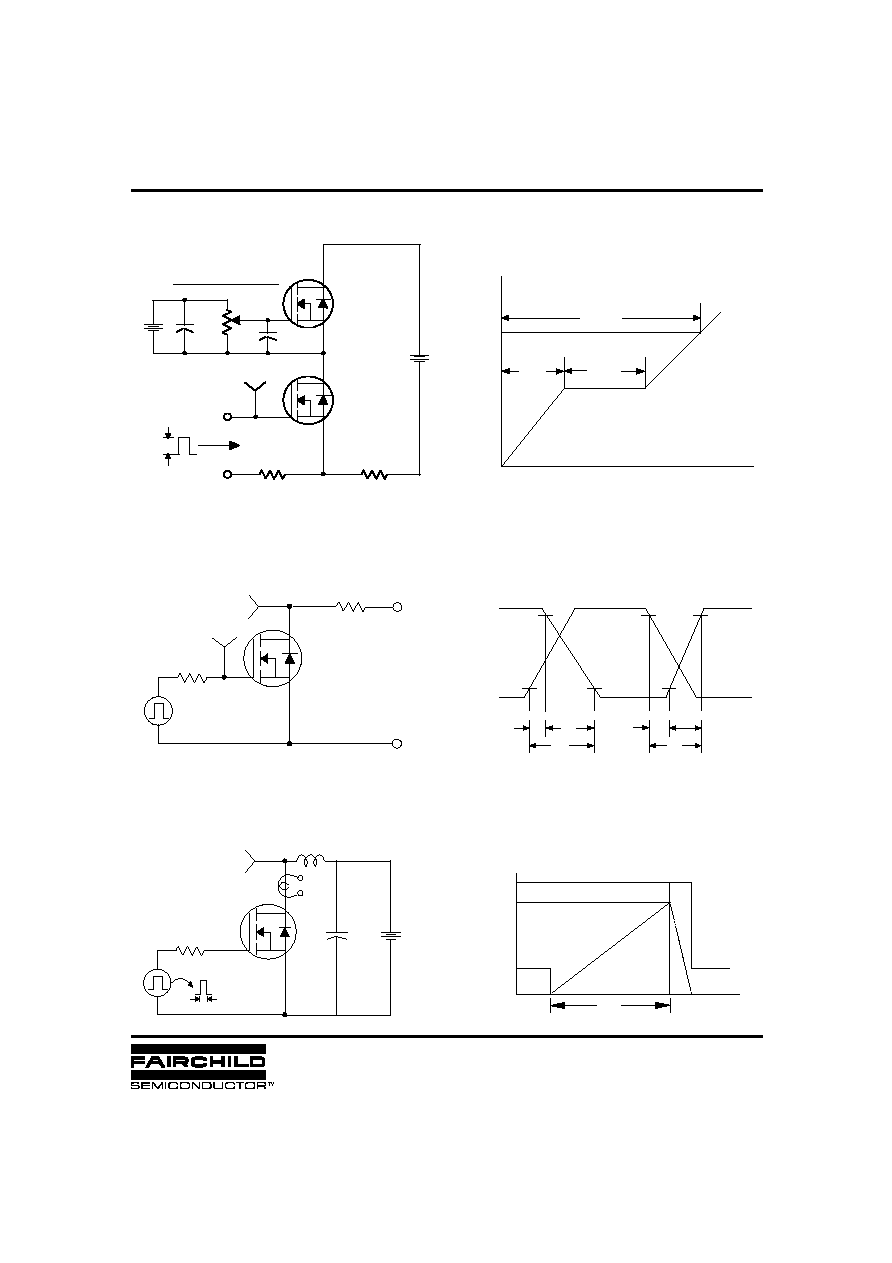
Fig 12. Gate Charge Test Circuit & Waveform
Fig 13. Resistive Switching Test Circuit & Waveforms
Fig 14. Unclamped Inductive Switching Test Circuit & Waveforms
E
AS
=
L
L
I
AS
2
----
2
1
--------------------
BV
DSS
-- V
DD
BV
DSS
V
in
V
out
10%
90%
t
d(on)
t
r
t
on
t
off
t
d(off)
t
f
Charge
V
GS
10V
Q
g
Q
gs
Q
gd
Vary t
p
to obtain
required peak I
D
10V
V
DD
C
L
L
V
DS
I
D
R
G
t
p
DUT
BV
DSS
t
p
V
DD
I
AS
V
DS
(t)
I
D
(t)
Time
V
DD
( 0.5 rated V
DS
)
10V
V
out
V
in
R
L
DUT
R
G
V
DS
3mA
V
GS
Current Sampling (I
G
)
Resistor
Current Sampling (I
D
)
Resistor
DUT
300nF
50K
200nF
12V
Same Type
as DUT
" Current Regulator "
R
1
R
2
SSF17N60A