 | –≠–ª–µ–∫—Ç—Ä–æ–Ω–Ω—ã–π –∫–æ–º–ø–æ–Ω–µ–Ω—Ç: SSH7N90A | –°–∫–∞—á–∞—Ç—å:  PDF PDF  ZIP ZIP |
1
FEATURES
∑
Avalanche Rugged Technology
∑
Rugged Gate Oxide Technology
∑
Lower Input Capacitance
∑
Improved Gate Charge
∑
Extended Safe Operating Area
∑
Lower Leakage Current: 25
µ
A (Max.) @ V
DS
= 900V
∑
Lower R
DS(ON)
: 1.247
(Typ.)
ABSOLUTE MAXIMUM RATINGS
THERMAL RESISTANCE
Symbol
Characteristics
Value
Units
V
DSS
Drain-to-Source Voltage
900
V
I
D
Continuous Drain Current (T
C
= 25
∞
C)
7
A
Continuous Drain Current (T
C
= 100
∞
C)
4.4
I
DM
Drain Current-Pulsed
28
A
V
GS
Gate-to-Source Voltage
±
30
V
E
AS
Single Pulsed Avalanche Energy
778
mJ
I
AR
Avalanche Current
7
A
E
AR
Repetitive Avalanche Energy
24
mJ
dv/dt
Peak Diode Recovery dv/dt
1.5
V/ns
P
D
Total Power Dissipation (T
C
= 25
∞
C)
Linear Derating Factor
240
1.92
W
W/
∞
C
T
J
, T
STG
Operating Junction and Storage
Temperature Range
-
55 to +150
∞
C
T
L
Maximum Lead Temp. for Soldering
Purposes, 1/8" from case for 5-seconds
300
Symbol
Characteristics
Typ.
Max.
Units
R
JC
Junction-to-Case
-
0.52
∞
C/W
R
CS
Case-to-Sink
0.24
-
R
JA
Junction-to-Ambient
-
40
BV
DSS
= 900V
R
DS(ON)
= 1.8
I
D
= 7A
TO-3P
1. Gate 2. Drain 3. Source
3
2
1
N-CHANNEL POWER MOSFET
SSH7N90A
1999 Fairchild Semiconductor Corporation
REV. B
x
y
x
x
z
SSH7N90A
N-CHANNEL POWER MOSFET
2
ELECTRICAL CHARACTERISTICS
(T
C
= 25
∞
C unless otherwise specified)
SOURCE-DRAIN DIODE RATINGS AND CHARACTERISTICS
Notes:
x
Repetitive Rating: Pulse Width Limited by Maximum Junction Temperature
y
L=30mH, I
AS
=7A, V
DD
=50V, R
G
=27
, Starting T
J
=25
∞
C
z
I
SD
8A, di/dt
170A/
µ
s, V
DD
BV
DSS
, Starting T
J
=25
∞
C
{
Pulse Test: Pulse Width
250
µ
s, Duty Cycle
2%
|
Essentially Independent of Operating Temperature
Symbol
Characteristics
Min.
Typ.
Max.
Units
Test Conditions
BV
DSS
Drain-Source Breakdown Voltage
900
-
-
V
V
GS
=0V, I
D
=250
µ
A
BV/
T
J
Breakdown Voltage Temp. Coeff.
-
1.06
-
V/
∞
C
I
D
=250
µ
A, See Fig 7
V
GS(th)
Gate Threshold Voltage
2.0
-
3.5
V
V
DS
=5V, I
D
=250
µ
A
I
GSS
Gate-Source Leakage, Forward
-
-
100
nA
V
GS
=30V
Gate-Source Leakage, Reverse
-
-
-
100
V
GS
=
-
30V
I
DSS
Drain-to-Source Leakage Current
-
-
25
µ
A
V
DS
=900V
-
-
250
V
DS
=720V, T
C
=125
∞
C
R
DS(on)
Static Drain-Source
On-State Resistance
-
-
1.8
V
GS
=10V, I
D
=3.5A
{
g
fs
Forward Transconductance
-
5.8
-
S
V
DS
=50V, I
D
=3.5A
{
C
iss
Input Capacitance
-
2070
2690
pF
V
GS
=0V, V
DS
=25V
f=1MHz
See Fig 5
C
oss
Output Capacitance
-
185
215
C
rss
Reverse Transfer Capacitance
-
78
90
t
d(on)
Turn-On Delay Time
-
25
60
ns
V
DD
=450V, I
D
=8A
R
G
=10
See Fig 13
{ |
t
r
Rise Time
-
35
85
t
d(off)
Turn-Off Delay Time
-
122
255
t
f
Fall Time
-
41
90
Q
g
Total Gate Charge
-
94
123
nC
V
DS
=720V, V
GS
=10V
I
D
=8A
See Fig 6 & Fig 12
{ |
Q
gs
Gate-Source Charge
-
14.9
-
Q
gd
Gate-Drain (Miller) Charge
-
43.5
-
Symbol
Characteristics
Min.
Typ.
Max.
Units
Test Conditions
I
S
Continuous Source Current
-
-
7
A
Integral reverse pn-diode
in the MOSFET
I
SM
Pulsed-Source Current
x
-
-
28
V
SD
Diode Forward Voltage
{
-
-
1.4
V
T
J
=25
∞
C, I
S
=7A, V
GS
=0V
t
rr
Reverse Recovery Time
-
620
-
ns
T
J
=25
∞
C, I
F
=8A
di
F
/dt=100A/
µ
s
{
Q
rr
Reverse Recovery Charge
-
9.3
-
µ
C
3
10
-1
10
0
10
1
10
-1
10
0
10
1
@ Notes :
1. 250
µ
s Pulse Test
2. T
C
= 25
o
C
V
GS
Top : 1 5 V
1 0 V
8.0 V
7.0 V
6.0 V
5.5 V
5.0 V
Bottom : 4.5 V
I
D
, D
rai
n C
urre
nt
[A
]
V
DS
, Drain-Source Voltage [V]
2
4
6
8
10
10
-1
10
0
10
1
25
o
C
150
o
C
- 55
o
C
@ Notes :
1. V
GS
= 0 V
2. V
DS
= 50 V
3. 250
µ
s Pulse Test
I
D
, Drain Current [A]
V
GS
, Gate-Source Voltage [V]
0.2
0.4
0.6
0.8
1.0
1.2
10
-1
10
0
10
1
150
o
C
25
o
C
@ Notes :
1. V
GS
= 0 V
2. 250
µ
s Pulse Test
I
DR
, Reverse Drain Current [A]
V
SD
, Source-Drain Voltage [V]
0
5
10
15
20
25
30
35
0
1
2
3
4
5
@ Note : T
J
= 25
o
C
V
GS
= 20 V
V
GS
= 10 V
R
DS(
on)
,
[
]
D
rai
n-S
our
ce O
n-R
esi
stan
ce
I
D
, Drain Current [A]
10
0
10
1
0
1000
2000
3000
C
iss
= C
gs
+ C
gd
(
C
ds
= shorted
)
C
oss
= C
ds
+ C
gd
C
rss
= C
gd
@ Notes :
1. V
GS
= 0 V
2. f = 1 MHz
C
rss
C
oss
C
iss
C
apa
cit
anc
e [
pF]
V
DS
, Drain-Source Voltage [V]
0
20
40
60
80
100
0
5
10
V
DS
= 720 V
V
DS
= 450 V
V
DS
= 180 V
@ Notes : I
D
= 8.0 A
V
GS
, Gate-Source Voltage [V]
Q
G
, Total Gate Charge [nC]
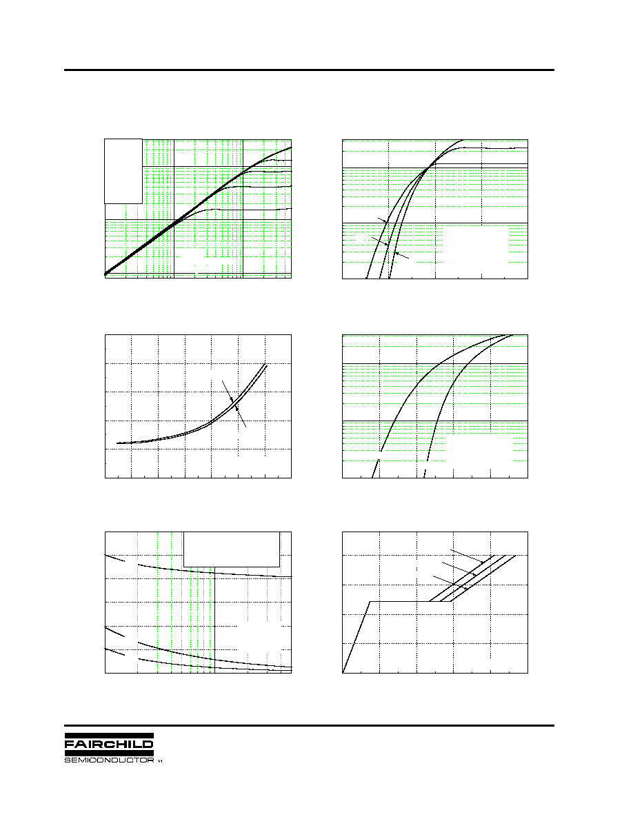
Fig 1. Output Characteristics
Fig 2. Transfer Characteristics
Fig 6. Gate Charge vs. Gate-Source Voltage
Fig 5. Capacitance vs. Drain-Source Voltage
Fig 4. Source-Drain Diode Forward Voltage
Fig 3. On-Resistance vs. Drain Current
N-CHANNEL POWER MOSFET
SSH7N90A
SSH7N90A
N-CHANNEL POWER MOSFET
4
-75
-50
-25
0
25
50
75
100
125
150
175
0.8
0.9
1.0
1.1
1.2
@ Notes :
1. V
GS
= 0 V
2. I
D
= 250
µ
A
BV
DSS
,
(No
rmal
ized)
D
rain-
Sour
ce Br
eakdo
wn Vo
ltage
T
J
, Junction Temperature [
o
C]
-75
-50
-25
0
25
50
75
100
125
150
175
0.0
0.5
1.0
1.5
2.0
2.5
3.0
@ Notes :
1. V
GS
= 10 V
2. I
D
= 4.0 A
R
DS
(o
n)
, (N
ormalized)
Drain
-Source On
-Resistan
ce
T
J
, Junction Temperature [
o
C]
25
50
75
100
125
150
0
2
4
6
8
I
D
, Dr
ain Curren
t [A]
T
c
, Case Temperature [
o
C]
10
1
10
2
10
3
10
-2
10
-1
10
0
10
1
10
2
100
µ
s
DC
10
µ
s
1 ms
10 ms
@ Notes :
1. T
C
= 25
o
C
2. T
J
= 150
o
C
3. Single Pulse
Operation in This Area
is Limited by R
DS(on)
I
D
, Dra
in C
urren
t [A
]
V
DS
, Drain-Source Voltage [V]
10
- 5
10
- 4
10
- 3
10
- 2
10
- 1
10
0
10
1
10
- 2
10
- 1
single pulse
0.2
0.1
0.01
0.02
0.05
D=0.5
@ Notes :
1. Z
J C
(t)=0.52
o
C/W Max.
2. Duty Factor, D=t
1
/t
2
3. T
J M
-T
C
=P
D M
*Z
J C
(t)
Z
JC
(
t) ,
The
rma
l Res
pon
se
t
1
, Square Wave Pulse Duration [sec]
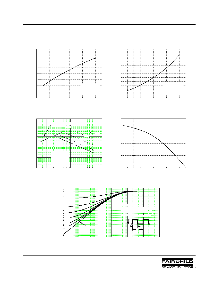
Fig 7. Breakdown Voltage vs. Temperature
Fig 8. On-Resistance vs. Temperature
Fig 11. Thermal Response
Fig 10. Max. Drain Current vs. Case Temperature
Fig 9. Max. Safe Operating Area
P
DM
t
1
t
2
5
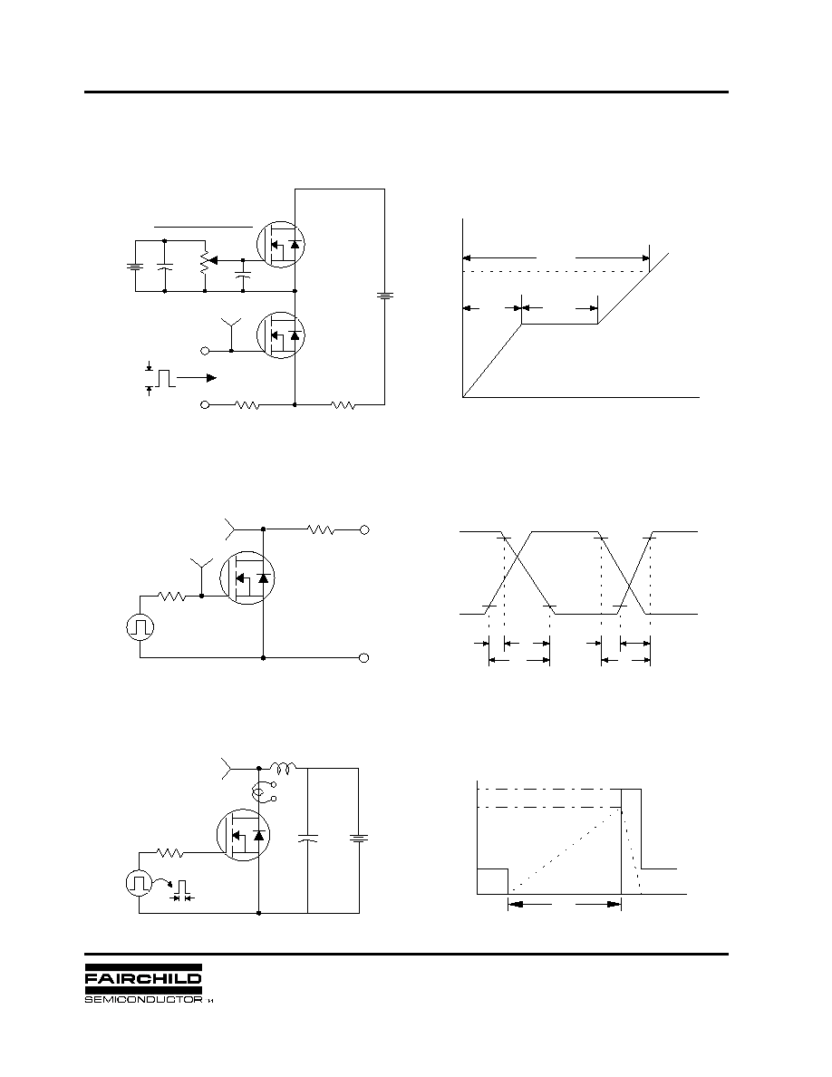
Fig 12. Gate Charge Test Circuit & Waveform
Fig 13. Resistive Switching Test Circuit & Waveforms
Fig 14. Unclamped Inductive Switching Test Circuit & Waveforms
E
AS
=
L
L
I
AS
2
----
2
1
--------------------
BV
DSS
-- V
DD
BV
DSS
V
in
V
out
10%
90%
t
d(on)
t
r
t
on
t
off
t
d(off)
t
f
Charge
V
GS
10V
Q
g
Q
gs
Q
gd
Vary t
p
to obtain
required peak I
D
10V
V
DD
C
L
L
V
DS
I
D
R
G
t
p
DUT
BV
DSS
t
p
V
DD
I
AS
V
DS
(t)
I
D
(t)
Time
V
DD
( 0.5 rated V
DS
)
10V
V
out
V
in
R
L
DUT
R
G
3mA
V
GS
Current Sampling (I
G
)
Resistor
Current Sampling (I
D
)
Resistor
DUT
V
DS
300nF
50K
200nF
12V
Same Type
as DUT
Current Regulator
R
1
R
2
N-CHANNEL POWER MOSFET
SSH7N90A
SSH7N90A
N-CHANNEL POWER MOSFET
6
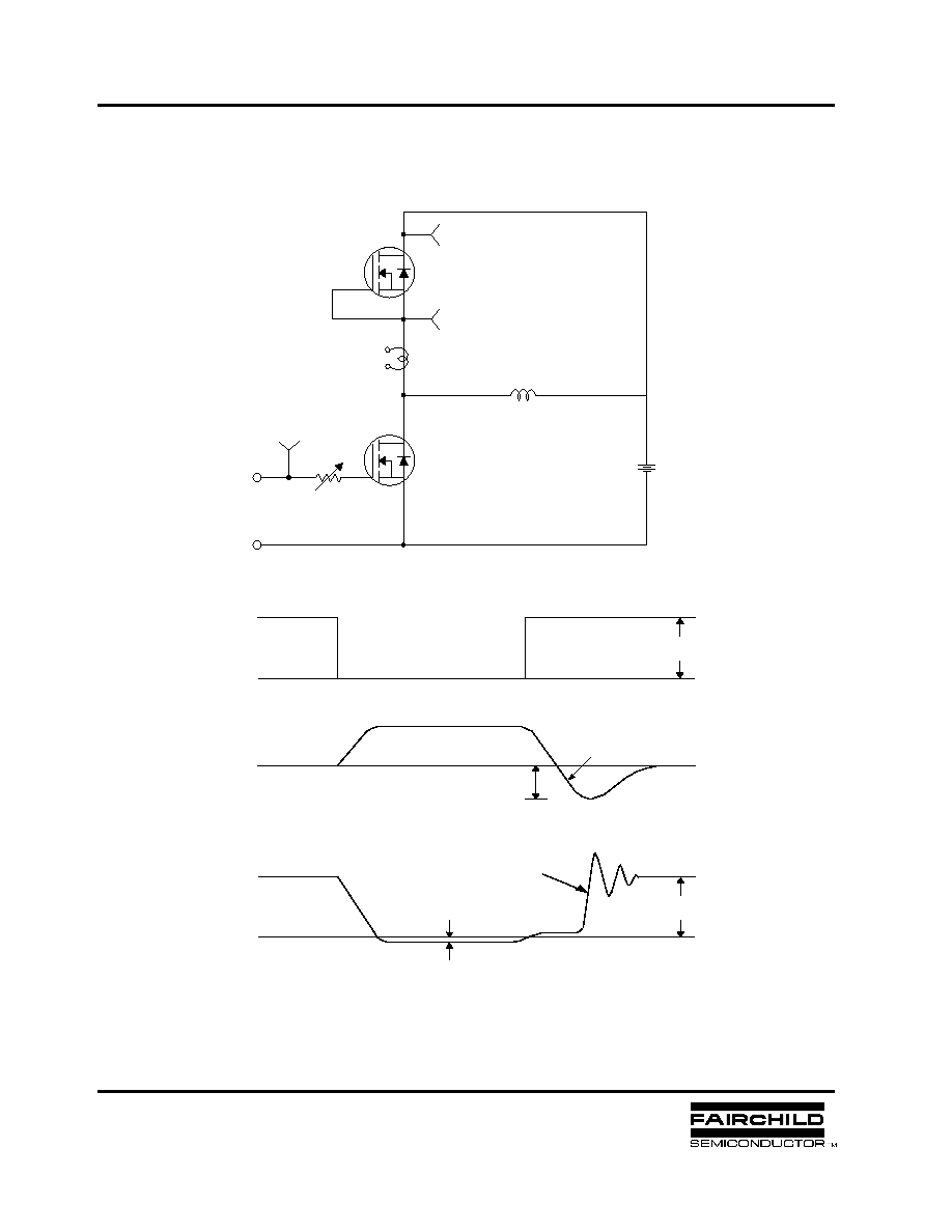
Fig 15. Peak Diode Recovery dv/dt Test Circuit & Waveforms
DUT
V
DS
+
--
L
I
S
Driver
V
GS
R
G
Same Type
as DUT
V
GS
∑ dv/dt controlled by
G
∑ I
S
controlled by Duty Factor
?
V
DD
10V
V
GS
( Driver )
I
S
( DUT )
V
DS
( DUT )
V
DD
Body Diode
Forward Voltage Drop
V
f
I
FM
, Body Diode Forward Current
Body Diode Reverse Current
I
RM
Body Diode Recovery dv/dt
di/dt
D =
Gate Pulse Width
Gate Pulse Period
--------------------------
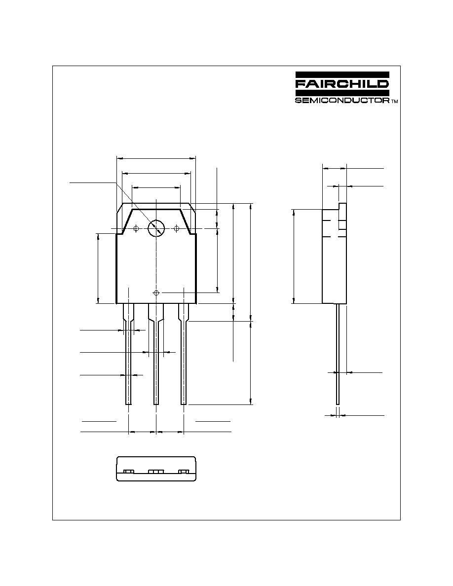
Dimensions in Millimeters
August 1999, Rev B
TO-3P Package Dimensions
15.60
±
0.20
4.80
±
0.20
13.60
±
0.20
9.60
±
0.20
2.00
±
0.20
3.00
±
0.20
1.00
±
0.20
1.40
±
0.20
¯3.20
±
0.10
3.80
±
0.20
13.90
±
0.20
3.50
±
0.20
16.50
±
0.30
12.76
±
0.20
19.90
±
0.20
23.40
±
0.20
18.70
±
0.20
1.50
+0.15
≠0.05
0.60
+0.15
≠0.05
5.45TYP
[5.45
±
0.30
]
5.45TYP
[5.45
±
0.30
]
TO-3P (FS PKG CODE AF)

TRADEMARKS
ACExTM
CoolFETTM
CROSSVOLTTM
E
2
CMOS
TM
FACTTM
FACT Quiet SeriesTM
FAST
Æ
FASTrTM
GTOTM
HiSeCTM
The following are registered and unregistered trademarks Fairchild Semiconductor owns or is authorized to use and is
not intended to be an exhaustive list of all such trademarks.
LIFE SUPPORT POLICY
FAIRCHILD'S PRODUCTS ARE NOT AUTHORIZED FOR USE AS CRITICAL COMPONENTS IN LIFE SUPPORT
DEVICES OR SYSTEMS WITHOUT THE EXPRESS WRITTEN APPROVAL OF FAIRCHILD SEMICONDUCTOR CORPORATION.
As used herein:
1. Life support devices or systems are devices or
systems which, (a) are intended for surgical implant into
the body, or (b) support or sustain life, or (c) whose
failure to perform when properly used in accordance
with instructions for use provided in the labeling, can be
reasonably expected to result in significant injury to the
user.
2. A critical component is any component of a life
support device or system whose failure to perform can
be reasonably expected to cause the failure of the life
support device or system, or to affect its safety or
effectiveness.
PRODUCT STATUS DEFINITIONS
Definition of Terms
Datasheet Identification
Product Status
Definition
Advance Information
Preliminary
No Identification Needed
Obsolete
This datasheet contains the design specifications for
product development. Specifications may change in
any manner without notice.
This datasheet contains preliminary data, and
supplementary data will be published at a later date.
Fairchild Semiconductor reserves the right to make
changes at any time without notice in order to improve
design.
This datasheet contains final specifications. Fairchild
Semiconductor reserves the right to make changes at
any time without notice in order to improve design.
This datasheet contains specifications on a product
that has been discontinued by Fairchild semiconductor.
The datasheet is printed for reference information only.
Formative or
In Design
First Production
Full Production
Not In Production
DISCLAIMER
FAIRCHILD SEMICONDUCTOR RESERVES THE RIGHT TO MAKE CHANGES WITHOUT FURTHER
NOTICE TO ANY PRODUCTS HEREIN TO IMPROVE RELIABILITY, FUNCTION OR DESIGN. FAIRCHILD
DOES NOT ASSUME ANY LIABILITY ARISING OUT OF THE APPLICATION OR USE OF ANY PRODUCT
OR CIRCUIT DESCRIBED HEREIN; NEITHER DOES IT CONVEY ANY LICENSE UNDER ITS PATENT
RIGHTS, NOR THE RIGHTS OF OTHERS.
TinyLogicTM
UHCTM
VCXTM
ISOPLANARTM
MICROWIRETM
POPTM
PowerTrenchTM
QFETTM
QSTM
Quiet SeriesTM
SuperSOTTM-3
SuperSOTTM-6
SuperSOTTM-8