 | ÐлекÑÑоннÑй компоненÑ: SSI6N70A | СкаÑаÑÑ:  PDF PDF  ZIP ZIP |
SSW/I6N70A N-Channel Power MOSFET
1
FEATURES
·
Avalanche Rugged Technology
·
Rugged Gate Oxide Technology
·
Lower Input Capacitance
·
Improved Gate Charge
·
Extended Safe Operating Area
·
Lower Leakage Current: 25
µ
A (Max.) @ V
DS
= 800V
·
Lower R
DS(ON)
: 1.552
(Typ.)
ABSOLUTE MAXIMUM RATINGS
THERMAL RESISTANCE
* When mounted on the minimum pad size recommended (PCB Mount.)
Symbol
Characteristics
Value
Units
V
DSS
Drain-to-Source Voltage
700
V
I
D
Continuous Drain Current (T
C
= 25
°
C)
6
A
Continuous Drain Current (T
C
= 100
°
C)
3.8
I
DM
Drain Current-Pulsed
24
A
V
GS
Gate-to-Source Voltage
±
30
V
E
AS
Single Pulsed Avalanche Energy
582
mJ
I
AR
Avalanche Current
6
A
E
AR
Repetitive Avalanche Energy
13
mJ
dv/dt
Peak Diode Recovery dv/dt
2.5
V/ns
P
D
Total Power Dissipation (T
A
= 25
°
C) *
3.1
W
Total Power Dissipation (T
C
= 25
°
C)
Linear Derating Factor
130
1.04
W
W/
°
C
T
J
, T
STG
Operating Junction and Storage
Temperature Range
-
55 to +150
°
C
T
L
Maximum Lead Temp. for Soldering
Purposes, 1/8" from case for 5-seconds
300
Symbol
Characteristics
Typ.
Max.
Units
R
JC
Junction-to-Case
-
0.52
°
C/W
R
JA
Junction-to-Ambient *
-
40
R
JA
Junction-to-Ambient
-
62.5
BV
DSS
= 700V
R
DS(ON)
= 1.8
I
D
= 6A
D2-PAK
1. Gate 2. Drain 3. Source
I2-PAK
N-CHANNEL POWER MOSFET
SSW/I6N70A
1999 Fairchild Semiconductor Corporation
REV. B
x
y
x
x
z
SSW/I6N70A
N-CHANNEL POWER MOSFET
2
ELECTRICAL CHARACTERISTICS
(T
C
= 25
°
C unless otherwise specified)
SOURCE-DRAIN DIODE RATINGS AND CHARACTERISTICS
Notes:
x
Repetitive Rating: Pulse Width Limited by Maximum Junction Temperature
y
L=30mH, I
AS
=6A, V
DD
=50V, R
G
=27
, Starting T
J
=25
°
C
z
I
SD
6A, di/dt
140A/
µ
s, V
DD
BV
DSS
, Starting T
J
=25
°
C
{
Pulse Test: Pulse Width
250
µ
s, Duty Cycle
2%
|
Essentially Independent of Operating Temperature
Symbol
Characteristics
Min.
Typ.
Max.
Units
Test Conditions
BV
DSS
Drain-Source Breakdown Voltage
700
-
-
V
V
GS
=0V, I
D
=250
µ
A
BV/
T
J
Breakdown Voltage Temp. Coeff.
-
0.79
-
V/
°
C
I
D
=250
µ
A, See Fig 7
V
GS(th)
Gate Threshold Voltage
2.0
-
4.0
V
V
DS
=5V, I
D
=250
µ
A
I
GSS
Gate-Source Leakage, Forward
-
-
100
nA
V
GS
=30V
Gate-Source Leakage, Reverse
-
-
-
100
V
GS
=
-
30V
I
DSS
Drain-to-Source Leakage Current
-
-
25
µ
A
V
DS
=700V
-
-
250
V
DS
=560V, T
C
=125
°
C
R
DS(on)
Static Drain-Source
On-State Resistance
-
-
1.8
V
GS
=10V, I
D
=3A
{
g
fs
Forward Transconductance
-
4.12
-
S
V
DS
=50V, I
D
=3A
{
C
iss
Input Capacitance
-
920
1200
pF
V
GS
=0V, V
DS
=25V
f=1MHz
See Fig 5
C
oss
Output Capacitance
-
100
115
C
rss
Reverse Transfer Capacitance
-
45
55
t
d(on)
Turn-On Delay Time
-
18
45
ns
V
DD
=350V, I
D
=6A
R
G
=11.5
See Fig 13
{ |
t
r
Rise Time
-
23
55
t
d(off)
Turn-Off Delay Time
-
76
160
t
f
Fall Time
-
26
60
Q
g
Total Gate Charge
-
51
67
nC
V
DS
=560V, V
GS
=10V
I
D
=6A
See Fig 6 & Fig 12
{ |
Q
gs
Gate-Source Charge
-
8.3
-
Q
gd
Gate-Drain (Miller) Charge
-
23.1
-
Symbol
Characteristics
Min.
Typ.
Max.
Units
Test Conditions
I
S
Continuous Source Current
-
-
6
A
Integral reverse pn-diode
in the MOSFET
I
SM
Pulsed-Source Current
x
-
-
24
V
SD
Diode Forward Voltage
{
-
-
1.4
V
T
J
=25
°
C, I
S
=6A, V
GS
=0V
t
rr
Reverse Recovery Time
-
440
-
ns
T
J
=25
°
C, I
F
=6A
di
F
/dt=100A/
µ
s
{
Q
rr
Reverse Recovery Charge
-
4.05
-
µ
C
3
10
-1
10
0
10
1
10
-1
10
0
10
1
@ Notes :
1. 250
µ
s Pulse Test
2. T
C
= 25
o
C
V
GS
Top : 1 5 V
1 0 V
8.0 V
7.0 V
6.0 V
5.5 V
5.0 V
Bottom : 4.5 V
I
D
, D
rai
n C
urre
nt
[A
]
V
DS
, Drain-Source Voltage [V]
2
4
6
8
10
10
-1
10
0
10
1
25
o
C
150
o
C
- 55
o
C
@ Notes :
1. V
GS
= 0 V
2. V
DS
= 50 V
3. 250
µ
s Pulse Test
I
D
, Drain Current [A]
V
GS
, Gate-Source Voltage [V]
0
5
10
15
20
0
2
4
6
@ Note : T
J
= 25
o
C
V
GS
= 20 V
V
GS
= 10 V
R
DS(
on)
,
[
]
D
rai
n-S
our
ce O
n-R
esi
stan
ce
I
D
, Drain Current [A]
0.2
0.4
0.6
0.8
1.0
1.2
10
-1
10
0
10
1
150
o
C
25
o
C
@ Notes :
1. V
GS
= 0 V
2. 250
µ
s Pulse Test
I
DR
, Reverse Drain Current [A]
V
SD
, Source-Drain Voltage [V]
10
0
10
1
0
500
1000
1500
C
iss
= C
gs
+ C
gd
(
C
ds
= shorted
)
C
oss
= C
ds
+ C
gd
C
rss
= C
gd
@ Notes :
1. V
GS
= 0 V
2. f = 1 MHz
C
rss
C
oss
C
iss
C
apa
cit
anc
e [
pF]
V
DS
, Drain-Source Voltage [V]
0
10
20
30
40
50
60
0
5
10
V
DS
= 560 V
V
DS
= 350 V
V
DS
= 140 V
@ Notes : I
D
= 6.0 A
V
GS
, Gate-Source Voltage [V]
Q
G
, Total Gate Charge [nC]
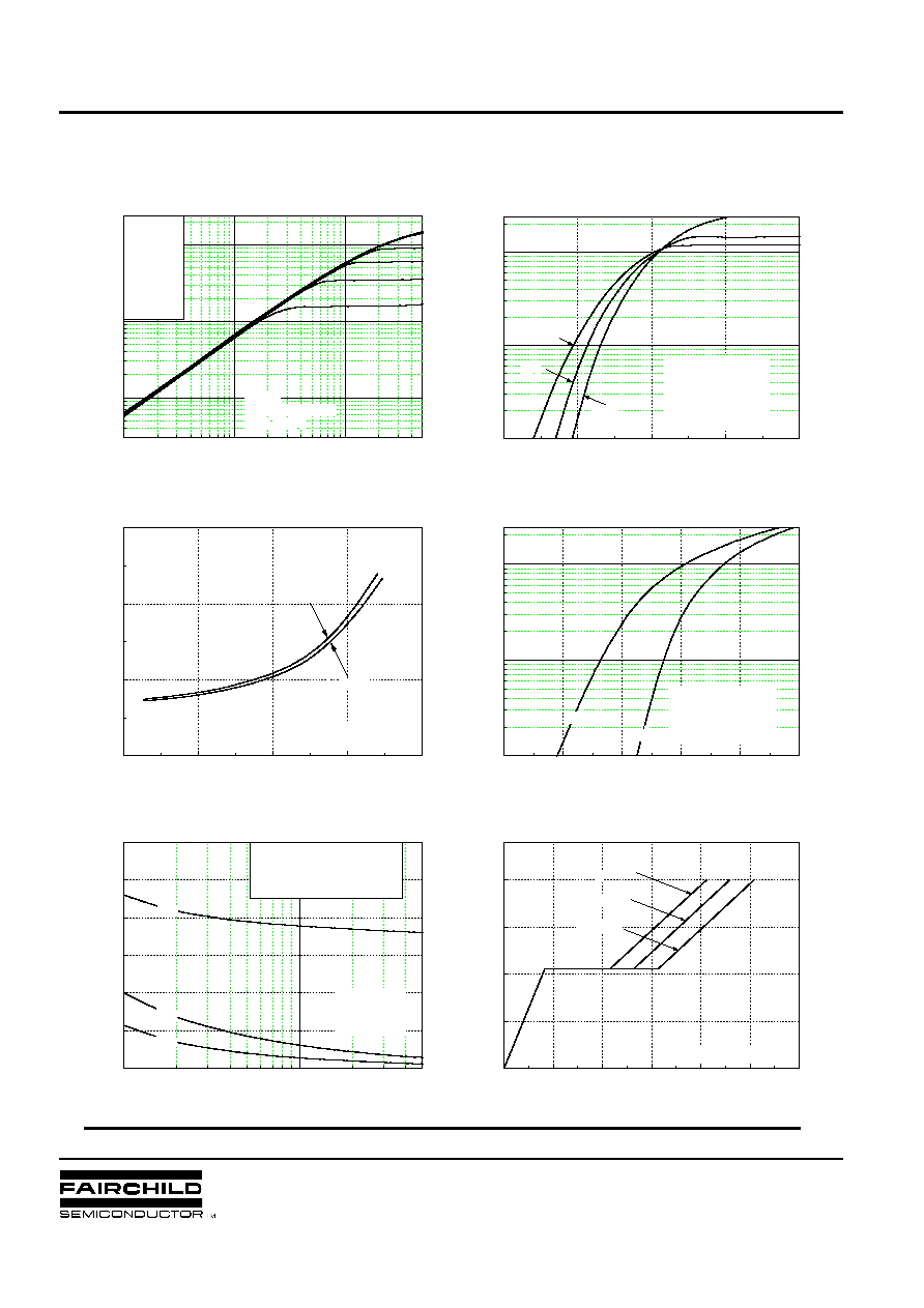
Fig 1. Output Characteristics
Fig 2. Transfer Characteristics
Fig 6. Gate Charge vs. Gate-Source Voltage
Fig 5. Capacitance vs. Drain-Source Voltage
Fig 4. Source-Drain Diode Forward Voltage
Fig 3. On-Resistance vs. Drain Current
N-CHANNEL POWER MOSFET
SSH8N80A
SSW/I6N70A
N-CHANNEL POWER MOSFET
4
-75
-50
-25
0
25
50
75
100
125
150
175
0.8
0.9
1.0
1.1
1.2
@ Notes :
1. V
GS
= 0 V
2. I
D
= 250
µ
A
BV
DSS
,
(No
rmal
ized)
D
rain-
Sour
ce Br
eakdo
wn Vo
ltage
T
J
, Junction Temperature [
o
C]
-75
-50
-25
0
25
50
75
100
125
150
175
0.0
0.5
1.0
1.5
2.0
2.5
3.0
@ Notes :
1. V
GS
= 10 V
2. I
D
= 3.0 A
R
DS
(o
n)
, (N
ormalized)
Drain
-Source On
-Resistan
ce
T
J
, Junction Temperature [
o
C]
10
1
10
2
10
3
10
-2
10
-1
10
0
10
1
10
2
10
µ
s
DC
100
µ
s
1 ms
10 ms
@ Notes :
1. T
C
= 25
o
C
2. T
J
= 150
o
C
3. Single Pulse
Operation in This Area
is Limited by R
DS(on)
I
D
, Dra
in C
urren
t [A
]
V
DS
, Drain-Source Voltage [V]
25
50
75
100
125
150
0
2
4
6
8
I
D
, Dr
ain Curren
t [A]
T
c
, Case Temperature [
o
C]
10
- 5
10
- 4
10
- 3
10
- 2
10
- 1
10
0
10
1
10
- 2
10
- 1
10
0
single pulse
0.2
0.1
0.01
0.02
0.05
D=0.5
@ Notes :
1. Z
J C
(t)=0.96
o
C/W Max.
2. Duty Factor, D=t
1
/t
2
3. T
J M
-T
C
=P
D M
*Z
J C
(t)
Z
JC
(
t) ,
The
rma
l Res
pon
se
t
1
, Square Wave Pulse Duration [sec]
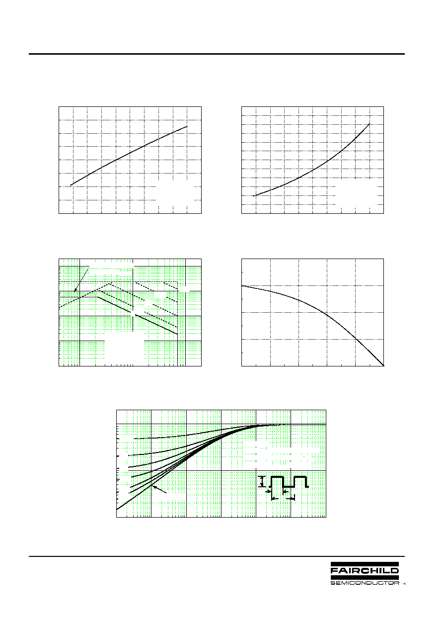
Fig 7. Breakdown Voltage vs. Temperature
Fig 8. On-Resistance vs. Temperature
Fig 11. Thermal Response
Fig 10. Max. Drain Current vs. Case Temperature
Fig 9. Max. Safe Operating Area
P
DM
t
1
t
2
5
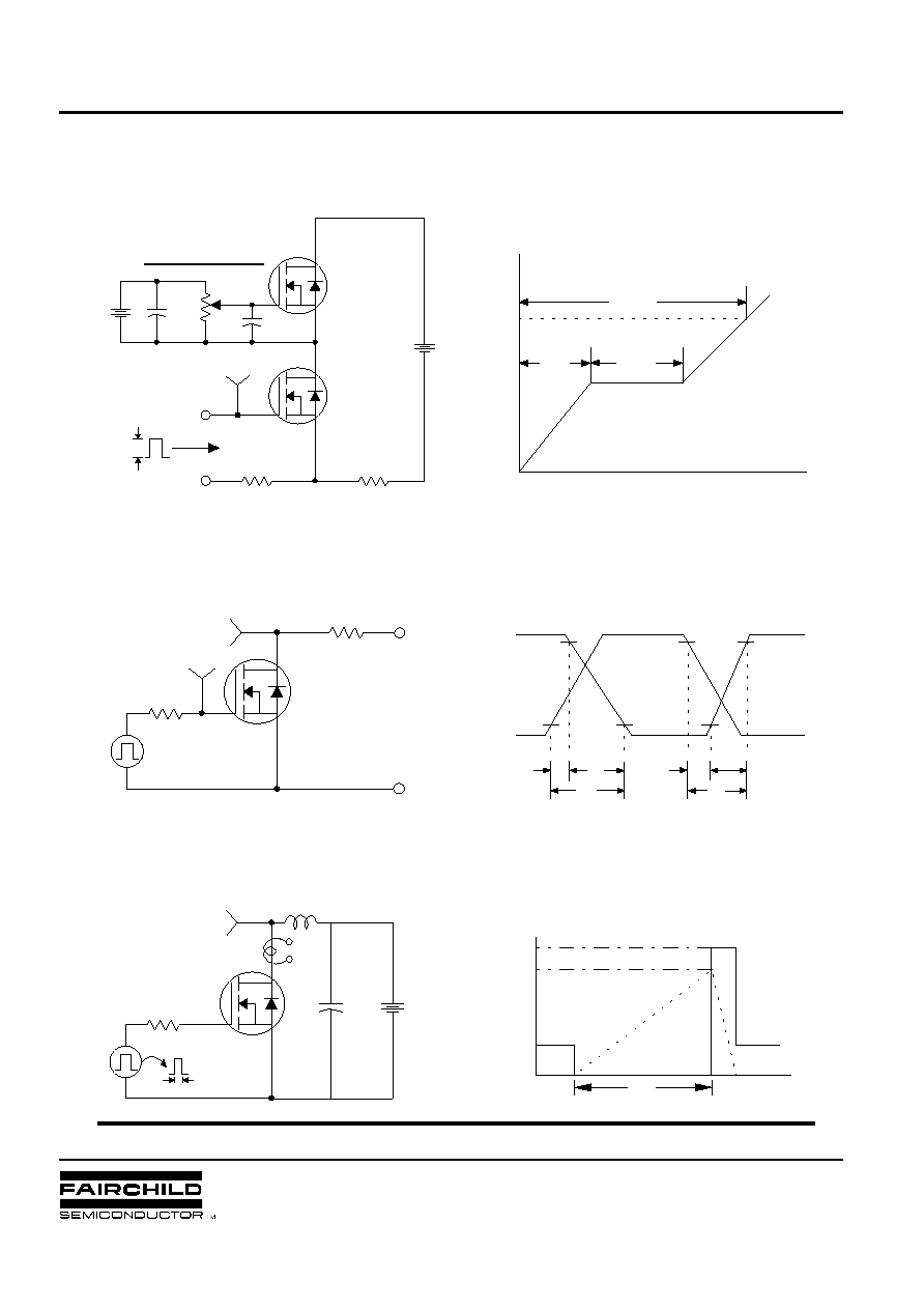
Fig 12. Gate Charge Test Circuit & Waveform
Fig 13. Resistive Switching Test Circuit & Waveforms
Fig 14. Unclamped Inductive Switching Test Circuit & Waveforms
E
AS
=
L
L
I
AS
2
----
2
1
--------------------
BV
DSS
-- V
DD
BV
DSS
V
in
V
out
10%
90%
t
d(on)
t
r
t
on
t
off
t
d(off)
t
f
Charge
V
GS
10V
Q
g
Q
gs
Q
gd
Vary t
p
to obtain
required peak I
D
10V
V
DD
C
L
L
V
DS
I
D
R
G
t
p
DUT
BV
DSS
t
p
V
DD
I
AS
V
DS
(t)
I
D
(t)
Time
V
DD
( 0.5 rated V
DS
)
10V
V
out
V
in
R
L
DUT
R
G
3mA
V
GS
Current Sampling (I
G
)
Resistor
Current Sampling (I
D
)
Resistor
DUT
V
DS
300nF
50K
200nF
12V
Same Type
as DUT
Current Regulator
R
1
R
2
N-CHANNEL POWER MOSFET
SSW/I6N70A