Avalanche Rugged Technology
Rugged Gate Oxide Technology
Lower Input Capacitance
Improved Gate Charge
Extended Safe Operating Area
Lower Leakage Current : 25
µ
A (Max.) @ V
DS
= 900V
Low R
DS(ON)
: 2.300
(Typ.)
Advanced Power MOSFET
Thermal Resistance
Junction-to-Case
Case-to-Sink
Junction-to-Ambient
R
JC
R
CS
R
JA
C
/W
Characteristic
Max.
Units
Symbol
Typ.
FEATURES
Absolute Maximum Ratings
Drain-to-Source Voltage
Continuous Drain Current (T
C
=25
C
)
Continuous Drain Current (T
C
=100
C
)
Drain Current-Pulsed
Gate-to-Source Voltage
Single Pulsed Avalanche Energy
Avalanche Current
Repetitive Avalanche Energy
Peak Diode Recovery dv/dt
Total Power Dissipation (T
C
=25
C
)
Linear Derating Factor
Operating Junction and
Storage Temperature Range
Maximum Lead Temp. for Soldering
Purposes, 1/8 " from case for 5-seconds
Characteristic
Value
Units
Symbol
I
DM
V
GS
E
AS
I
AR
E
AR
dv/dt
I
D
P
D
T
J
, T
STG
T
L
A
V
mJ
A
mJ
V/ns
W
W/
C
A
C
V
DSS
V
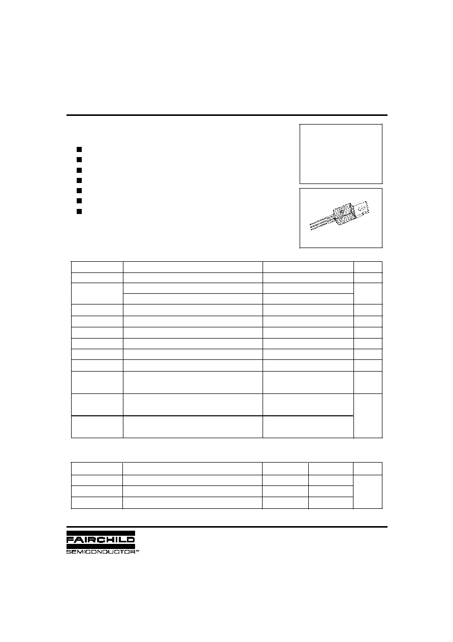
TO-220
1.Gate 2. Drain 3. Source
3
2
1
O
1
O
1
O
1
O
2
O
3
SSP5N90A
BV
DSS
= 900 V
R
DS(on)
= 2.9
I
D
= 5 A
900
5
3.2
20
529
5
14
1.5
140
1.12
- 55 to +150
300
0.89
--
62.5
--
0.5
--
30
+
_
©1999 Fairchild Semiconductor Corporation
Rev. B

N-CHANNEL
POWER MOSFET
Electrical Characteristics
(T
C
=25
C
unless otherwise specified)
Drain-Source Breakdown Voltage
Breakdown Voltage Temp. Coeff.
Gate Threshold Voltage
Gate-Source Leakage , Forward
Gate-Source Leakage , Reverse
Characteristic
Symbol
Max. Units
Typ.
Min.
Test Condition
Static Drain-Source
On-State Resistance
Forward Transconductance
Input Capacitance
Output Capacitance
Reverse Transfer Capacitance
Turn-On Delay Time
Rise Time
Turn-Off Delay Time
Fall Time
Total Gate Charge
Gate-Source Charge
Gate-Drain( "Miller" ) Charge
g
fs
C
iss
C
oss
C
rss
t
d(on)
t
r
t
d(off)
t
f
Q
g
Q
gs
Q
gd
BV
DSS
BV/
T
J
V
GS(th)
R
DS(on)
I
GSS
I
DSS
V
V/
C
V
nA
µ
A
pF
ns
nC
--
--
--
--
--
--
--
--
--
--
--
--
--
V
GS
=0V,I
D
=250
µ
A
I
D
=250
µ
A See Fig 7
V
DS
=5V,I
D
=250
µ
A
V
GS
=30V
V
GS
=-30V
V
DS
=900V
V
DS
=720V,T
C
=125
C
V
GS
=10V,I
D
=2.5A
*
V
DS
=50V,I
D
=2.5A
V
DD
=450V,I
D
=5A,
R
G
=13.6
See Fig 13
V
DS
=720V,V
GS
=10V,
I
D
=5A
See Fig 6 & Fig 12
Drain-to-Source Leakage Current
V
GS
=0V,V
DS
=25V,f =1MHz
See Fig 5
Source-Drain Diode Ratings and Characteristics
Continuous Source Current
Pulsed-Source Current
Diode Forward Voltage
Reverse Recovery Time
Reverse Recovery Charge
I
S
I
SM
V
SD
t
rr
Q
rr
Characteristic
Symbol
Max. Units
Typ.
Min.
Test Condition
--
--
--
--
--
A
V
ns
µ
C
Integral reverse pn-diode
in the MOSFET
T
J
=25
C
,I
S
=5A,V
GS
=0V
T
J
=25
C
,I
F
=5A
di
F
/dt=100A/
µ
s
O
4
O
4
O
4
O
5
O
5
O
4
O
4
O
4
O
1
SSP5N90A
900
--
2.0
--
--
--
--
--
1.14
--
--
--
--
--
105
43
21
39
94
32
54
9.0
25.0
--
--
3.5
100
-100
25
250
2.9
--
1440
125
50
50
90
200
75
70
--
--
4.0
1110
--
--
--
540
5.62
5
20
1.4
--
--
Notes ;
Repetitive Rating : Pulse Width Limited by Maximum Junction Temperature
L=40mH, I
AS
=5A, V
DD
=50V, R
G
=27
, Starting T
J
=25
C
I
SD
5A, di/dt 120A/
µ
s, V
DD
BV
DSS
, Starting T
J
=25
C
Pulse Test : Pulse Width = 250
µ
s, Duty Cycle 2%
Essentially Independent of Operating Temperature
<
_
<
_
<
_
<
_
O
1
O
2
O
3
O
4
O
5