 | ÐлекÑÑоннÑй компоненÑ: SSW1N50B | СкаÑаÑÑ:  PDF PDF  ZIP ZIP |
Äîêóìåíòàöèÿ è îïèñàíèÿ www.docs.chipfind.ru
©2002 Fairchild Semiconductor Corporation
Rev. C, May 2002
S
S
W1N50B /
SSI
1N50B
SSW1N50B / SSI1N50B
520V N-Channel MOSFET
General Description
These N-Channel enhancement mode power field effect
transistors are produced using Fairchild's proprietary,
planar, DMOS technology.
This advanced technology has been especially tailored to
minimize on-state resistance, provide superior switching
performance, and withstand high energy pulse in the
avalanche and commutation mode. These devices are well
suited for high efficiency switch mode power supplies,
power factor correction and electronic lamp ballasts based
on half bridge.
Features
· 1.5A, 520V, R
DS(on)
= 5.3
@V
GS
= 10 V
· Low gate charge ( typical 8.3 nC)
· Low Crss ( typical 5.5 pF)
· Fast switching
· 100% avalanche tested
· Improved dv/dt capability
Absolute Maximum Ratings
T
C
= 25°C unless otherwise noted
Thermal Characteristics
* When mounted on the minimum pad size recommended (PCB Mount)
Symbol
Parameter
SSW1N50B / SSI1N50B
Units
V
DSS
Drain-Source Voltage
520
V
I
D
Drain Current
- Continuous (T
C
= 25°C)
1.5
A
- Continuous (T
C
= 100°C)
0.97
A
I
DM
Drain Current
- Pulsed
(Note 1)
5.0
A
V
GSS
Gate-Source Voltage
±
30
V
E
AS
Single Pulsed Avalanche Energy
(Note 2)
100
mJ
I
AR
Avalanche Current
(Note 1)
1.5
A
E
AR
Repetitive Avalanche Energy
(Note 1)
3.6
mJ
dv/dt
Peak Diode Recovery dv/dt
(Note 3)
5.5
V/ns
P
D
Power Dissipation (T
A
= 25°C) *
3.13
W
Power Dissipation (T
C
= 25°C)
36
W
- Derate above 25°C
0.29
W/°C
T
J
, T
stg
Operating and Storage Temperature Range
-55 to +150
°C
T
L
Maximum lead temperature for soldering purposes,
1/8
"
from case for 5 seconds
300
°C
Symbol
Parameter
Typ
Max
Units
R
JC
Thermal Resistance, Junction-to-Case
--
3.44
°C
/
W
R
JA
Thermal Resistance, Junction-to-Ambient *
--
40
°C
/
W
R
JA
Thermal Resistance, Junction-to-Ambient
--
62.5
°C
/
W
!
!
!
!
!
!
!
!
!
!
!
!
!
!
!
!
!
!
!
!
!
!
!
!
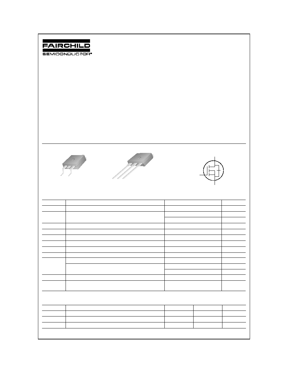
S
D
G
D
2
-PAK
SSW Series
I
2
-PAK
SSI Series
G
S
D
G
S
D
Rev. C, May 2002
S
S
W1N50B /
SSI
1N50B
©2002 Fairchild Semiconductor Corporation
Electrical Characteristics
T
C
= 25°C unless otherwise noted
Notes:
1. Repetitive Rating : Pulse width limited by maximum junction temperature
2. L = 80mH, I
AS
= 1.5A, V
DD
= 50V, R
G
= 25
,
Starting T
J
= 25°C
3. I
SD
1.5A, di/dt
300A/
µ
s, V
DD
BV
DSS,
Starting T
J
= 25°C
4. Pulse Test : Pulse width
300
µ
s, Duty cycle
2%
5. Essentially independent of operating temperature
Symbol
Parameter
Test Conditions
Min
Typ
Max
Units
Off Characteristics
BV
DSS
Drain-Source Breakdown Voltage
V
GS
= 0 V, I
D
= 250
µ
A
520
--
--
V
BV
DSS
/
T
J
Breakdown Voltage Temperature
Coefficient
I
D
= 250
µ
A, Referenced to 25°C
--
0.54
--
V/°C
I
DSS
Zero Gate Voltage Drain Current
V
DS
= 520 V, V
GS
= 0 V
--
--
10
µ
A
V
DS
= 400 V, T
C
= 125°C
--
--
100
µ
A
I
GSSF
Gate-Body Leakage Current, Forward
V
GS
= 30 V, V
DS
= 0 V
--
--
100
nA
I
GSSR
Gate-Body Leakage Current, Reverse
V
GS
= -30 V, V
DS
= 0 V
--
--
-100
nA
On Characteristics
V
GS(th)
Gate Threshold Voltage
V
DS
= V
GS
, I
D
= 250
µ
A
2.0
--
4.0
V
R
DS(on)
Static Drain-Source
On-Resistance
V
GS
= 10 V, I
D
= 0.75 A
--
4.1
5.3
g
FS
Forward Transconductance
V
DS
= 40 V, I
D
= 0.75 A
(Note4)
--
1.8
--
S
Dynamic Characteristics
C
iss
Input Capacitance
V
DS
= 25 V, V
GS
= 0 V,
f = 1.0 MHz
--
260
340
pF
C
oss
Output Capacitance
--
25
33
pF
C
rss
Reverse Transfer Capacitance
--
5.5
7.2
pF
Switching Characteristics
t
d(on)
Turn-On Delay Time
V
DD
= 250 V, I
D
= 1.5 A,
R
G
= 25
(Note4, 5)
--
14
40
ns
t
r
Turn-On Rise Time
--
40
90
ns
t
d(off)
Turn-Off Delay Time
--
35
80
ns
t
f
Turn-Off Fall Time
--
35
80
ns
Q
g
Total Gate Charge
V
DS
= 400 V, I
D
= 1.5 A,
V
GS
= 10 V
(Note4, 5)
--
8.3
11
nC
Q
gs
Gate-Source Charge
--
1.5
--
nC
Q
gd
Gate-Drain Charge
--
3.4
--
nC
Drain-Source Diode Characteristics and Maximum Ratings
I
S
Maximum Continuous Drain-Source Diode Forward Current
--
--
1.5
A
I
SM
Maximum Pulsed Drain-Source Diode Forward Current
--
--
5.0
A
V
SD
Drain-Source Diode Forward Voltage
V
GS
= 0 V, I
S
= 1.5 A
--
--
1.4
V
t
rr
Reverse Recovery Time
V
GS
= 0 V, I
S
= 1.5 A,
dI
F
/ dt = 100 A/
µ
s
(Note4)
--
230
--
ns
Q
rr
Reverse Recovery Charge
--
0.94
--
µ
C
Rev. C, May 2002
S
S
W1N50B /
SSI
1N50B
©2002 Fairchild Semiconductor Corporation
0.2
0.4
0.6
0.8
1.0
1.2
1.4
10
-1
10
0
150
Notes :
1. V
GS
= 0V
2. 250
s Pulse Test
25
I
DR
,
R
e
v
e
r
s
e D
r
ai
n C
u
r
r
en
t
[
A
]
V
SD
, Source-Drain voltage [V]
0
1
2
3
4
5
3
6
9
12
15
V
GS
= 20V
V
GS
= 10V
Note : T
J
= 25
R
DS
(
O
N
)
[
],
D
r
ai
n-
Sour
c
e
O
n
-
R
es
i
s
t
a
nc
e
I
D
, Drain Current [A]
2
4
6
8
10
10
-1
10
0
150
o
C
25
o
C
-55
o
C
Notes :
1. V
DS
= 40V
2. 250
s Pulse Test
I
D
,
D
r
ai
n C
u
r
r
e
nt
[
A
]
V
GS
, Gate-Source Voltage [V]
10
-1
10
0
10
1
10
-2
10
-1
10
0
V
GS
Top : 15.0 V
10.0 V
8.0 V
7.0 V
6.5 V
6.0 V
5.5 V
Bottom : 5.0 V
Notes :
1. 250
s Pulse Test
2. T
C
= 25
I
D
,
D
r
ai
n C
u
r
r
e
n
t
[
A
]
V
DS
, Drain-Source Voltage [V]
0.0
1.5
3.0
4.5
6.0
7.5
9.0
0
2
4
6
8
10
12
V
DS
= 250V
V
DS
= 100V
V
DS
= 400V
Note : I
D
= 1.5 A
V
GS
,
G
a
t
e
-
S
ou
r
c
e V
o
l
t
age [
V
]
Q
G
, Total Gate Charge [nC]
10
-1
10
0
10
1
0
100
200
300
400
500
C
oss
C
iss
= C
gs
+ C
gd
(C
ds
= shorted)
C
oss
= C
ds
+ C
gd
C
rss
= C
gd
Notes :
1. V
GS
= 0 V
2. f = 1 MHz
C
rss
C
iss
C
a
pac
i
t
an
c
e
[
p
F]
V
DS
, Drain-Source Voltage [V]
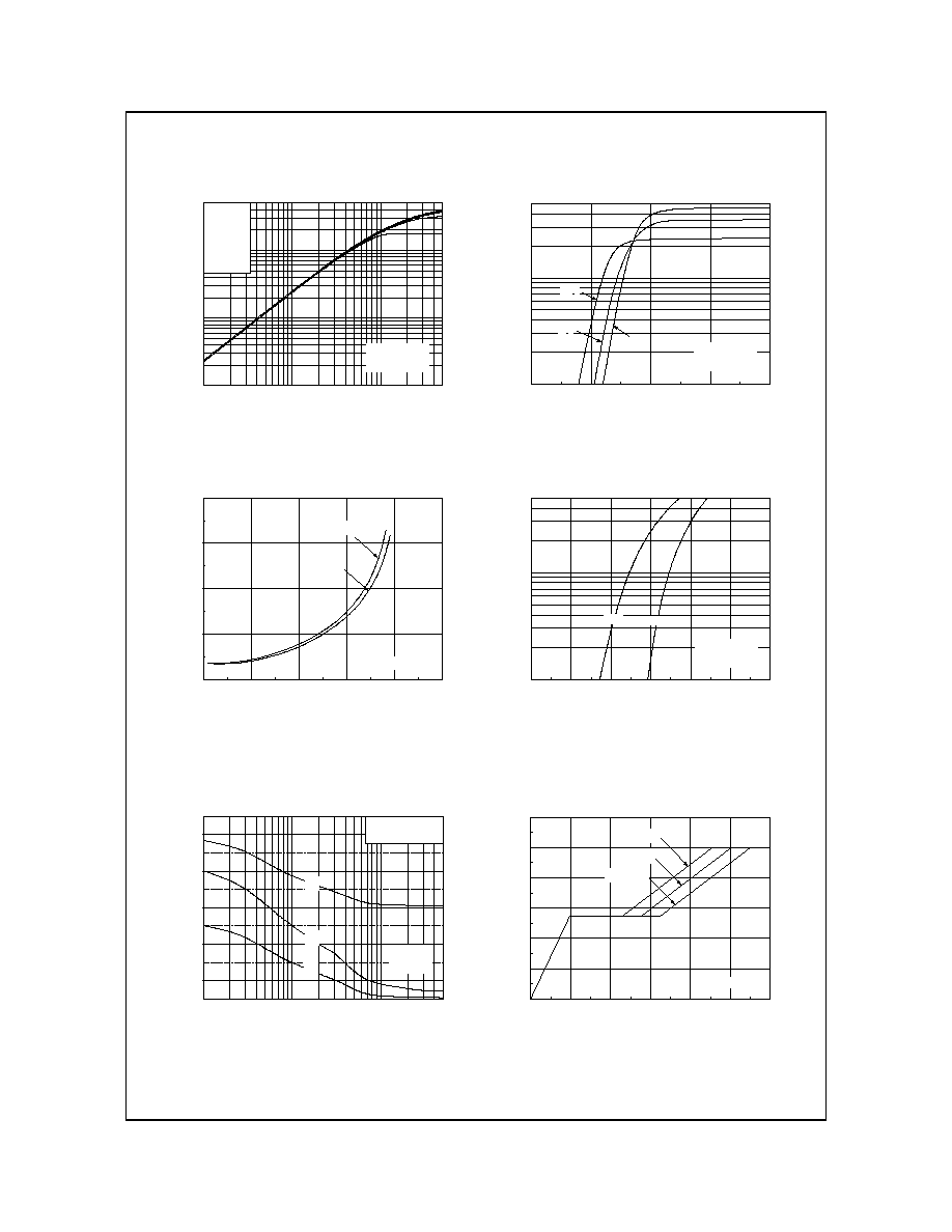
Typical Characteristics
Figure 5. Capacitance Characteristics
Figure 6. Gate Charge Characteristics
Figure 3. On-Resistance Variation vs
Drain Current and Gate Voltage
Figure 4. Body Diode Forward Voltage
Variation with Source Current
and Temperature
Figure 2. Transfer Characteristics
Figure 1. On-Region Characteristics
©2002 Fairchild Semiconductor Corporation
Rev. C, May 2002
S
S
W1N50B /
SSI
1N50B
-100
-50
0
50
100
150
200
0.0
0.5
1.0
1.5
2.0
2.5
3.0
Notes :
1. V
GS
= 10 V
2. I
D
= 0.75 A
R
DS
(
O
N
)
,
(
N
or
m
a
l
i
z
ed)
D
r
ai
n-
Sour
c
e
O
n
-
R
es
i
s
t
a
n
c
e
T
J
, Junction Temperature [
o
C]
-100
-50
0
50
100
150
200
0.8
0.9
1.0
1.1
1.2
Notes :
1. V
GS
= 0 V
2. I
D
= 250
A
BV
DS
S
,
(
N
o
r
m
a
liz
e
d
)
D
r
a
i
n-
S
o
ur
c
e
B
r
ea
k
d
o
w
n
V
o
l
t
ag
e
T
J
, Junction Temperature [
o
C]
1 0
-5
1 0
-4
1 0
-3
1 0
-2
1 0
-1
1 0
0
1 0
1
1 0
-1
1 0
0
N o te s :
1 . Z
J C
(t) = 3 .4 4
/W M a x .
2 . D u ty F a c to r, D = t
1
/t
2
3 . T
J M
- T
C
= P
D M
* Z
J C
(t)
s in g le p u ls e
D = 0 .5
0 .0 2
0 .2
0 .0 5
0 .1
0 .0 1
Z
JC
(t), T
h
e
r
m
a
l
R
e
s
p
o
n
s
e
t
1
, S q u a re W a v e P u ls e D u ra tio n [s e c ]
25
50
75
100
125
150
0.0
0.3
0.6
0.9
1.2
1.5
1.8
I
D
, D
r
a
i
n
C
u
r
r
e
n
t
[A
]
T
C
, Case Temperature [
]
10
0
10
1
10
2
10
3
10
-2
10
-1
10
0
10
1
DC
10 ms
1 ms
100
µ
s
Operation in This Area
is Limited by R
DS(on)
Notes :
1. T
C
= 25
o
C
2. T
J
= 150
o
C
3. Single Pulse
I
D
,
D
r
ai
n C
u
r
r
e
nt
[
A
]
V
DS
, Drain-Source Voltage [V]
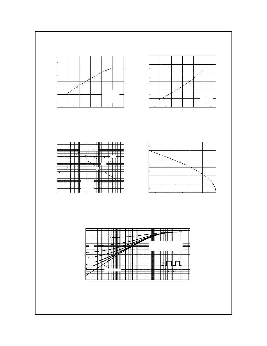
Typical Characteristics
(Continued)
Figure 9. Maximum Safe Operating Area
Figure 10. Maximum Drain Current
vs Case Temperature
Figure 7. Breakdown Voltage Variation
vs Temperature
Figure 8. On-Resistance Variation
vs Temperature
Figure 11. Transient Thermal Response Curve
t
1
P
DM
t
2
Rev. C, May 2002
S
S
W1N50B /
SSI
1N50B
©2002 Fairchild Semiconductor Corporation
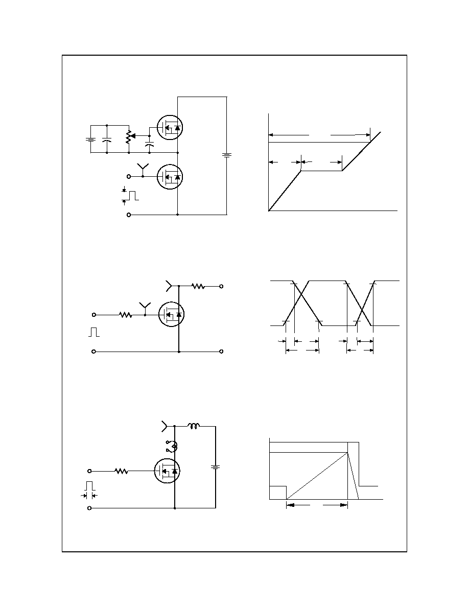
Charge
V
GS
10V
Q
g
Q
gs
Q
gd
3mA
V
GS
DUT
V
DS
300nF
50K
200nF
12V
Same Type
as DUT
Charge
V
GS
10V
Q
g
Q
gs
Q
gd
3mA
V
GS
DUT
V
DS
300nF
50K
200nF
12V
Same Type
as DUT
V
GS
V
DS
10%
90%
t
d(on)
t
r
t
on
t
off
t
d(off)
t
f
V
DD
10V
V
DS
R
L
DUT
R
G
V
GS
V
GS
V
DS
10%
90%
t
d(on)
t
r
t
on
t
off
t
d(off)
t
f
V
DD
10V
V
DS
R
L
DUT
R
G
V
GS
E
AS
=
L I
AS
2
----
2
1
--------------------
BV
DSS
- V
DD
BV
DSS
V
DD
V
DS
BV
DSS
t
p
V
DD
I
AS
V
DS
(t)
I
D
(t)
Time
10V
DUT
R
G
L
I
D
t
p
E
AS
=
L I
AS
2
----
2
1
E
AS
=
L I
AS
2
----
2
1
----
2
1
--------------------
BV
DSS
- V
DD
BV
DSS
V
DD
V
DS
BV
DSS
t
p
V
DD
I
AS
V
DS
(t)
I
D
(t)
Time
10V
DUT
R
G
L
L
I
D
I
D
t
p
Gate Charge Test Circuit & Waveform
Resistive Switching Test Circuit & Waveforms
Unclamped Inductive Switching Test Circuit & Waveforms