www.fairchildsemi.com
Features
· 4-bit resolution
· 1/4 LSB non-linearity
· Sample-and-hold circuit not required
· 25 Msps conversion rate
· Selectable output format
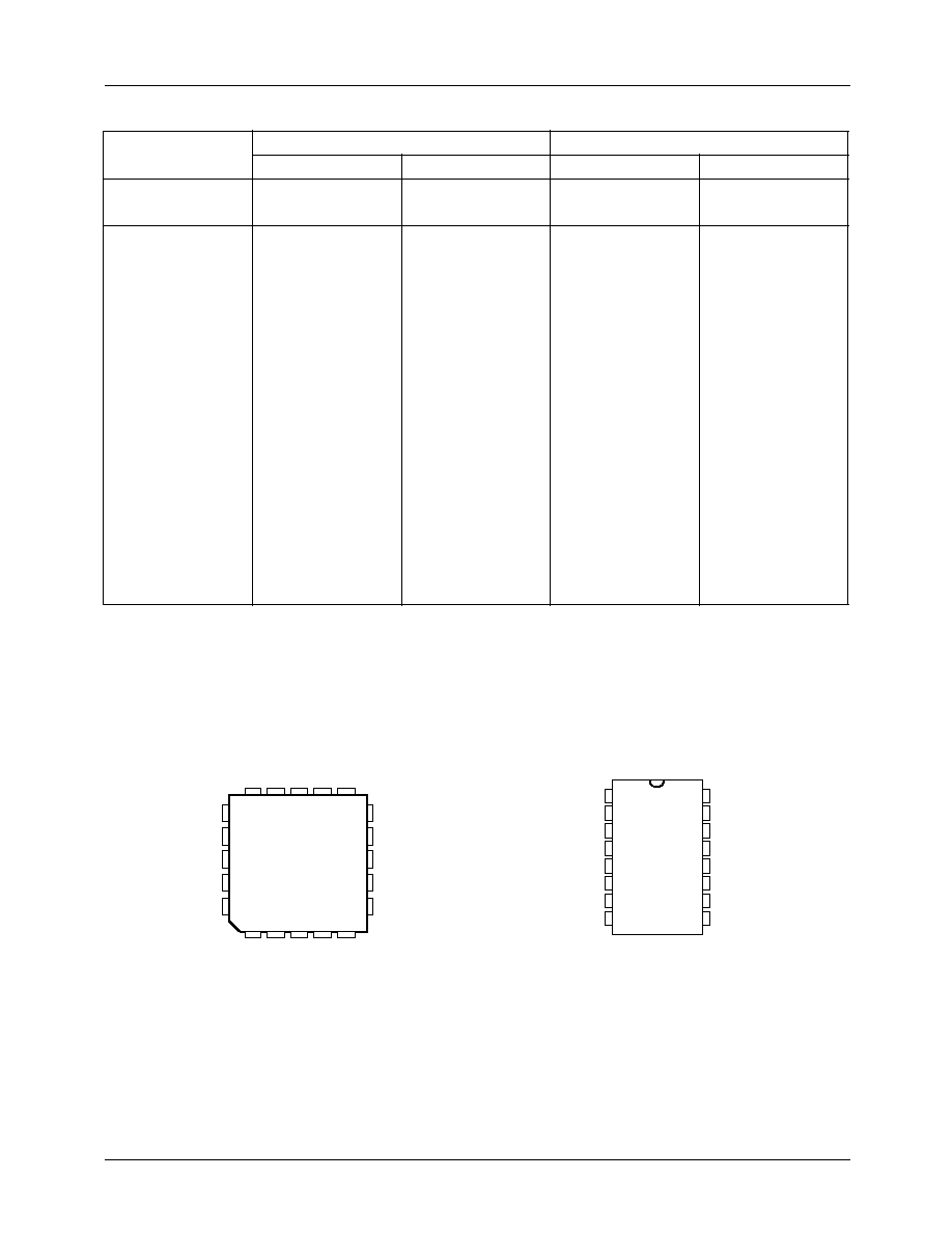
· 16-lead DIP and 20-lead PLCC packages
Applications
· Digital communications
· Video special effects
· Radar data conversion
· Medical imaging
Description
The TDC1044A is a 25 Msps (Megasample per second) full-
parallel analog-to-digital converter, capable of converting an
analog signal with full-power frequency components up to
12.5 MHz into 4-bit digital words. Use of a sample-and-hold
circuit is not necessary for operation of the TDC1044A. All
digital inputs and outputs are TTL compatible.
The TDC1044A consists of 15 latching comparators, encod-
ing logic, and an output register. A single convert signal
controls the conversion operation. Output formats are
true/inverted binary or true/inverted offset two's complement
codes.
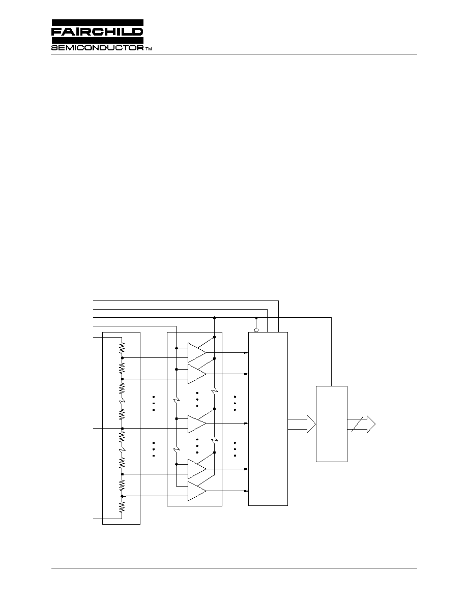
TDC1044A
Monolithic Video A/D Converter
4-Bit, 25 Msps
Block Diagram
R
1
R
M
R
T
V
IN
CONV
NLINV
NMINV
R
B
R
R
R
R
R
REFERENCE
RESISTOR
CHAIN
DIFFERENTIAL
COMPARATORS
(15)
15 TO 4
DECODER
LATCH
1
2
14
15
8
4
65-1044A-01
D
1
D
4
R
R/2
Rev. 1.1.2

TDC1044A
PRODUCT SPECIFICATION
2
Functional Description
General Information
The TDC1044A has three functional sections: a comparator
array, encoding logic, and an output register. The comparator
array compares the input signal with 15 reference voltages to
produce an N-of-15 thermometer code. All the comparators
referred to voltages more positive than the input signal will
be off, and those referred to voltages more negative than the
input signal will be on. Encoding logic converts the N-of-15
code into binary or two's complement coding and can invert
either output code. This coding function is controlled by DC
signals on pins NMINV and NLINV. The output register
holds the output constant between updates.
Power
The TDC1044A operates from two power supply voltages,
+5.0V and -5.2V. The return for I
CC
(the current drawn from
the +5.0V supply) is D
GND
. The return for I
EE
(the current
drawn from the -5.2V supply) is A
GND
. All power and
ground pins must be connected.
Reference
The TDC1044A converts analog signals in the range
V
RB
£
V
IN
£
V
RB
into digital form. V
RB
(the voltage
applied to R
B
at the bottom of the reference resistor chain)
and V
RT
(the voltage applied to R
B
at the top of the refer-
ence resistor chain) should be between +0.1V and -1.1V.
V
RT
should be more positive than V
RB
within that range.
The voltage applied across the reference resistor chain
(V
RT
V
RB
) must be between 0.4V and 1.3V.
Nominal voltages are V
RT
= 0.00V and V
RB
= -1.00V. These
voltages may be varied dynamically up to 10MHz. Due to
slight variation in the reference currents with clock and input
signals, R
T
and R
B
should be low-impedance points. For cir-
cuits in which the reference is not varied, a bypass capacitor
to ground is recommended. If the reference inputs are varied
dynamically (as in an Automatic Gain Control circuit), a
low-impedance reference source is required.
A reference middle, R
M
, is also provided; this may be used
as an input to adjust the mid-scale point in order to improve
integral linearity. This point may also be used as a tap to sup-
ply a mid-scale voltage to offset the analog input. If V
RM
is
used as an output, it must be connected to a high input
impedance device which has small input current. Noise at
this point may adversely affect the performance of this
device.
Controls
Two function control pins, NMINV and NLINV, set the out-
put format to be either straight binary or offset two's comple-
ment, in either true or inverted sense, according to Table 1.
These pins are active LOW as signified by the prefix "N" in
the signal name. They may be tied to VCC for a logic "1" and
DGND for a logic "0."
NMINV controls the MSB, D
1
; NLINV controls the three
LSBs: D
2
, D
3
and D
4
.
Convert
The TDC1044A requires a CONVert (CONV) signal. A sam-
ple is taken (the comparators are latched) within t
STO
after a
rising edge of CONV. The coded result is translated to the
output latches on the next rising edge. The outputs hold the
previous data a minimum time (t
HO
) after the rising edge of
the CONV signal. New data becomes valid after a maximum
delay time, t
D
.
Analog Input
The TDC1044A uses latching comparators which cause the
input impedance to vary slightly with the signal level. For
optimal performance, the source impedance of the driving
circuit must less than 25 Ohms. Within the range of V
EE
to
+0.5V, the input signal will not damage the device. If the
input signal is at a voltage between V
RT
and V
RB
, the output
will be a binary code between 0 and 15 inclusive. A signal
outside this range will indicate either full-scale positive or
full-scale negative, depending on whether the signal is off-
scale in the positive or negative direction.
Outputs
TDC1044A outputs are TTL compatible, and capable of
driving four low-power Schottky TTL (54/74 LS) unit loads.
The outputs hold the previous data a minimum time (t
HO
)
after the rising edge of the CONV signal. Data becomes
valid after a maximum delay time (t
D
) after the rising edge
of CONV. For optimum performance, 2.2 kOhm pull-up
resistors are recommended.
No Connects
Pin 3 of the TDC1044A is labeled No Connect (NC), and has
no connection to the chip. Connect this pin to A
GND
for best
noise performance.
PRODUCT SPECIFICATION
TDC1044A
5
Absolute Maximum Ratings
(beyond which the device may be damaged)
1
Notes:
1. Absolute maximum ratings are limiting values applied individually while all other parameters are within specified operating
conditions. Functional operation under any of these conditions is NOT implied.
2. Applied voltage must be current limited to specified range.
3. Forcing voltage must be limited to specified range.
4. Current is specified as positive when flowing into the device.
Operating Conditions
Type
Parameter
Min
Max
Unit
Supply Voltages
V
CC
(measured to D
GND
)
-0.5
7.0
V
V
EE
(measured to A
GND
)
+0.5
-7.0
V
A
GND
(measured to D
GND
)
-0.5
+0.5
V
Input Voltages
CONV, NMINV, NLINV (measured to D
GND
)
-0.5
+5.5
V
V
IN
, V
RT
, V
RB
(measured to A
GND
)
+0.5
V
EE
V
V
RT
(measured to V
RB
)
-2.2
+2.2
V
Output
Applied voltage (measured to D
GND
)
2
-0.5
+5.5
V
Applied current, externally forced
3,4
-1.0
+6.0
mA
Short circuit duration (single output in high state to ground)
1
sec
Temperature
Operating, ambient
-55
+125
°
C
Operating, junction
+150
°
C
Lead, soldering (10 seconds)
+300
°
C
Storage
-65
+150
°
C
Parameter
Min.
Nom.
Max.
Units
V
CC
Positive Supply Voltage (measured to D
GND
)
4.75
5.0
5.25
V
V
EE
Negative Supply Voltage (measured to A
GND
)
-4.9
-5.2
-5.5
V
V
AGND
Analog Ground Voltage (measured to D
GND
)
-0.1
0.0
0.1
V
t
PWL
CONV Pulse Width, LOW
17
ns
t
PWH
CONV Pulse Width, HIGH
17
ns
V
IL
Input Voltage, Logic LOW
0.8
V
V
IH
Input Voltage, Logic HIGH
2.0
V
I
OL
Output Current, Logic LOW
4.0
mA
I
OH
Output Current, Logic HIGH
-400
m
A
V
RT
Most Positive Reference
-1.9
0.0
0.1
V
V
RB
Most Negative Reference
-2.1
-1.0
-0.1
V
V
RT
V
RB
Reference Differential
0.2
1.0
2.0
V
V
IN
Input Voltage
V
RB
V
RT
V
T
A
Ambient Temperature, Still Air
0
70
°
C