
PRELIMINARY INFORMATION describes products that are not in full production at the time of printing. Specifications are based on design goals
and limited characterization. They may change without notice. Contact Fairchild Semiconductor for current information.
Pr
eliminar
y Infor
mation
www.fairchildsemi.com
Features
∑ 10-bit or 20-bit Parallel YCbCr input
∑ 24-bit RGB input
∑ D1, Genlock and Master mode operation
∑ Composite, S-video and component analog outputs
∑ Digital Composite output
∑ Fairchild demo board compatibility
Applications
∑ Evaluation of TMC2193 DENC
∑ Evaluation of TMC2072 Genlock interface
∑ Output for TMC2068P7C Decoder demo board
∑ System Breadboarding
Description
The TMB2193MS100 demonstration board provides a flexi-
ble base for evaluating the performance of the TMC2193
Digital Video Encoder (DENC). The demonstration board
can be driven by either a D1 or Genlock signal, or it can sup-
ply the synchronization signals needed to drive a framestore
or any MPEG Decoder. Both YCbCr, in either 4:2:2, D1, or
4:4:4 formats, and RGB inputs are supported. The board
provides high quality analog composite video, analog
S-video, analog component video and digital composite
video outputs.
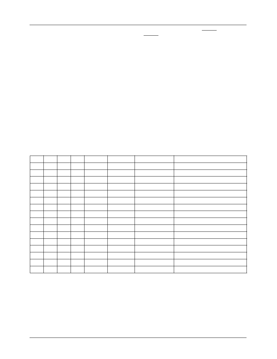
Block Diagram
96 Way
Edge
Connector
(female)
RBUS
Connector
1
32
65-B2193-01
Digital Inputs:
10 bit D1
24 bit RGB
20 bit YCbCr
PXCK
Analog Outputs:
Composite
S-Video
RGB
YPbPr
Sync
Digital Outputs (Optional):
10 bit DCVBS
HSYNC
VSYNC
PXCK
Digital Outputs:
HSYNC
VSYNC
MPXCK
TMC2193
FPGA
TMC2072
MCU
+5V 0V -5V
Analog
LPF
TMB2193MS100
Demonstration Board for the TMC2193
Rev. 0.9.0
TMB2193MS100
PRODUCT SPECIFICATION
2
Pr
eliminar
y Infor
mation
Functional Description
The TMB2193MS100 is designed to demonstrate the perfor-
mance of the TMC2193 Digital Video Encoder (DENC). For
a complete description of the TMC2193, please refer to the
TMC2193 data sheet. The TMB2193MS100 is compatible
with other Fairchild Demo boards. Typical configurations
are the TMC2067P7C, the TMC2068P7C, and the
TMB2193MS100 or the TMB0001MS100 and the
TMB2193MS100. The first configuration requires an analog
composite or S-video input and supplies a re-encoded analog
composite or S-video output. The later requires a parallel
D1 input and supplies an encoded analog composite or
S-video output.
The TMC2193 can be operated in D1, Genlock or Master
mode. In the D1 mode the synchronization is derived from
the TRS codes embedded in the D1 data stream. The
TMB2193MS100 has the TMC2072 Genlock front end,
which supplies the HSYNC, VSYNC and subcarrier infor-
mation to the TMC2193 for the Genlock operation of the
encoder. In Master mode the synchronization is driven by
the TMC2193, supplying the line (HSYNC) and field
(VSYNC or BnT) synchronization signals. With the
TMC2193 running in Master mode the TMB2193MS100
demo board interfaces directly to either a MPEG decoder or
a video framestore with no additional glue logic.
The TMB2193MS100 has an onboard microcontroller
(MCU) to program the TMC2193, the TMC2072, and to
configure the FPGA. All the default register maps are held
within the MCU. Table 1 provides a description of each of
the default register maps. A control register map is written to
the TMC2193, the TMC2072, and to Port 2 of the MCU each
time the MRST\ button is pressed. The MCU determines
which map to load from the PROG[3-0] (Px) dip switches.
The TMC2193, 2072 and the MCU can also be driven by the
Raydemo software. The interface is provided by the RBUS
connector on the TMB2193MS100 and the TMC2070P7C
R-Bus interface board. With this setup the user can config-
ure the TMC2193, the TMC2072 and the MCU with any
IBM compatible PC.
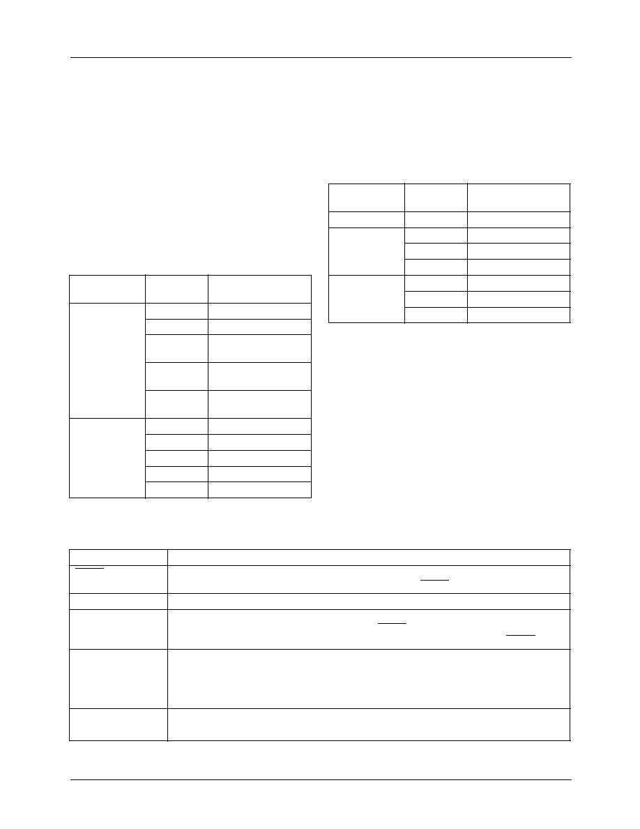
Table 1. Default Control Register Maps
P3
P2
P1
P0
Format
Mode
Source
Output Mode
0
0
0
0
NTSC
MASTER
Mod. Ramp
Composite, S-Video
0
0
0
1
NTSC
MASTER
75% CB
Composite, YPBPR
0
0
1
0
NTSC
MASTER
100% CB
Composite, RGB
0
0
1
1
NTSC
D1
D1
Composite, YPBPR
0
1
0
0
NTSC
D1
D1
Composite, RGB
0
1
0
1
NTSC
D1
D1
DCVBS
0
1
1
0
NTSC
Genlock
601
Composite, YPBPR
0
1
1
1
NTSC
Genlock
601
Composite, RGB
1
0
0
0
PAL
MASTER
Mod. Ramp
Composite, S-Video
1
0
0
1
PAL
MASTER
75% CB
Composite, YPBPR
1
0
1
0
PAL
MASTER
100% CB
Composite, RGB
1
0
1
1
PAL
D1
D1
Composite, YPBPR
1
1
0
0
PAL
D1
D1
Composite, RGB
1
1
0
1
PAL
D1
D1
DCVBS
1
1
1
0
PAL
Genlock
601
Composite, YPBPR
1
1
1
1
PAL
Genlock
601
Composite, RGB
PRODUCT SPECIFICATION
TMB2193MS100
3
Pr
eliminar
y Infor
mation
CPLD Description
The Altera 10K20 CLPD functions as the central matrix for
routing the buses to the TMC2193. Eight (8) control pins are
connected from port 2 of the MCU to the CLPD. These pins
are used to configure the CPLD and are broken up into 2
buses: FPGA control1 is on pins P2[7:4] and FPGA control2
is on pins P2[3:0]. The 10K20 default configuration routes
the 3 buses from the input edge connector and the bus from
the framestore header to the pixel data (PD[23:0]) port of the
TMC2193. This enables the various input formats of the
TMC2193 to be supported. In addition, the PD input can be
delayed in respect to the HSIN and VSIN for proper data
alignment. Table 2 describes the function of the pixel data
formatting.
The FPGA Control 2 bus selects which subcarrier reference
signal to be used; either the GRS from the TMC2072 or the
xRS signal from bus B of the input edge connector. FGPA
Control 2 also selects which set of synchronization signals
are to used; either the IXHSYNC and IXVSYNC from the
input edge connector or the TMC2072 GHSYNC and
GVSYNC.
FPGA Controls 1 and 2 can be accessed by the Raydemo
software. The dialog box exists in the MCU icon of the
TMB2193MS100 window. The functions of these controls
are purposely left generic to allow for the reconfiguration of
the CPLD.
The 10K20 utilization is approximately 20% of the available
logic cells. This allows for additional functions to be
implemented in the 10K20 such as notch filters, interpolation
filters for 4:2:2 to 4:4:4 conversion, simple comb filtering
and ancillary data insertion. These are just some of the
possibilities.
Table 2. FPGA Control 1
FGPA
Control1 bit#
Function
Description
3-2
PDMODE
PD Input
00
10-bit format, A bus
01
20-bit format, C and
B buses
10
24-bit format, C, A,
and B buses
11
10-bit format, A bus
delayed
1-0
PDDEL
PD delay
00
0 pxck's of delay
01
1 pxck's of delay
10
2 pxck's of delay
11
3 pxck's of delay
Table 3. FPGA Control 2
FGPA
Control2 bit#
Function
Description
3-2
No Modes
1
REFSEL
CVBS Input
0
B[5:2] bus
1
GENLOCK
0
SYNCSEL
HSIN, VSIN Input
0
IXH and IXV
1
GH and GV
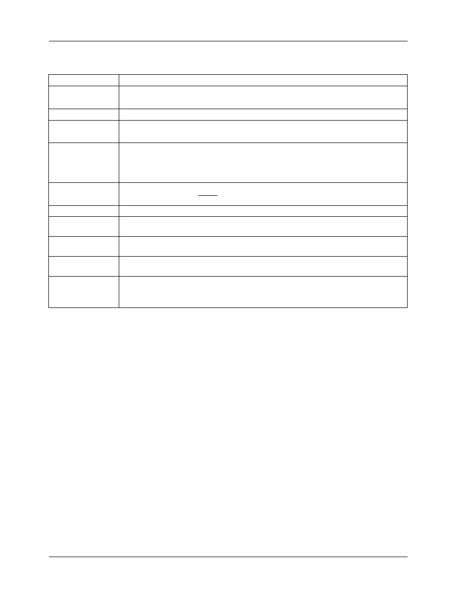
Table 4. Switch, Button, and Jumper Description
Button
Description
MRST
Resets the AT89C55. When the GLOBAL RESET jumper is in place, the reset line on all
boards connected to the TMB2193MS100 are driven by MRST.
Jumpers
Description
GLOBAL RESET
When GLOBAL RESET is open, only the TMC2193, the TMC2072, the framestore header
and the AT89C55 receive the reset pulse from MRST. When GLOBAL RESET is closed,
the reset line on all boards connected to the TMB2193MS100 are driven by MRST.
CASC INT
Cascade Programming Enable.
When CASC INT is open, the AT89C55 automatically initializes the devices after reset.
When CASC INT is closed, the AT89C55 will wait for a LOW pulse on the PGM_IN pin
before initializing the devices on the TMB2193MS100.
RBUSEN
When RBUSEN is open, the RBUS port is disabled.
When RBUSEN is closed, the RBUS port is enabled.
TMB2193MS100
PRODUCT SPECIFICATION
4
Pr
eliminar
y Infor
mation
Setup Procedure
Set E1 to MPXCK and E2 to PASS, enable the onboard TTL
clock oscillator as the clock source.
1.
Set ESA1-0 to ON (down).
2.
Set P3-0 to 0h, P3 is ON (down), P2 is ON (down), P1 is
ON (down), and P0 is ON (down).
3.
Plug in power supply connector and apply power. The
LED's corresponding to +5 Volts and -5 Volts should be
illuminated.
4.
Reset board by pressing the MRST button.
5.
Connect a scope probe to TP25 and adjust R39 until the
sync to blank amplitude is 286 mV.
6.
Connect a scope probe to TP19 and adjust R36 until the
sync to blank amplitude is 286 mV.
7.
Connect a scope probe to TP21 and adjust R37 until the
sync to blank amplitude is 286 mV.
8.
Connect a scope probe to TP23 and adjust R38 until the
burst amplitude is 286 mV.
Power Supply Requirements
The TMB2193MS100 board requires 1.5 Amps from the +5
Volt power supply and 0.5 Amps from the -5 Volt power sup-
ply. Both the +5 Volt and -5 Volt supplies are connected to
the input connector to supply the power requirements of any
upstream board. The +5 Volt power supply not only drives
TTL logic devices but it also provides the power and voltage
references to the D/A's in the TMC2193. Therefore, it is rec-
ommended that a bench power supply be used with the cable
lengths kept to a minimum.
JP20, JP21, JP22,
JP23
When JPx is open, the output video is a single 75Ohm termination.
When JPx is closed, the output video is a double 75Ohm termination.
Switches
Description
E1
Onboard Clock Selection.
Selects either the PXCK from the TMC2072 or the onboard TTL clock oscillator.
E2
Master Clock Selection.
When Pass is selected the clock source for the entire board is either the TMC2072 PXCK
or the TTL clock oscillator. When IXPCK is selected the clock source for the entire board
is the PXCK from the input header.
E3
Output Header Clock Selection.
Selects either PXCK or PXCK for the output header.
Dip Switches
Description
SA1-0
Configures the bits 2 and 1 of the TMC2193 RBUS chip address. When SAx is ON
(down), ESAx is in a LOW state. When SAx is OFF (up), ESAx is in a HIGH state.
CAS
Configures the bit 2 of the TMC2072 RBUS chip address. When CAS is ON (down),
GSA1 is in a LOW state. When CAS is OFF (up), GSA1 is in a HIGH state.
ERS
Configures the bit 1 of the TMC2072 RBUS chip address. When ERS is ON (down),
GSA0 is in a LOW state. When ERS is OFF (up), GSA0 is in a HIGH state.
P3-0
Control Register Programming.
P3-0 selects which control register map to configure the devices with. Refer to Table 1
Default Control Register Maps for a description.
Table 4. Switch, Button, and Jumper Description (continued)
Button
Description
PRODUCT SPECIFICATION
TMB2193MS100
5
Pr
eliminar
y Infor
mation
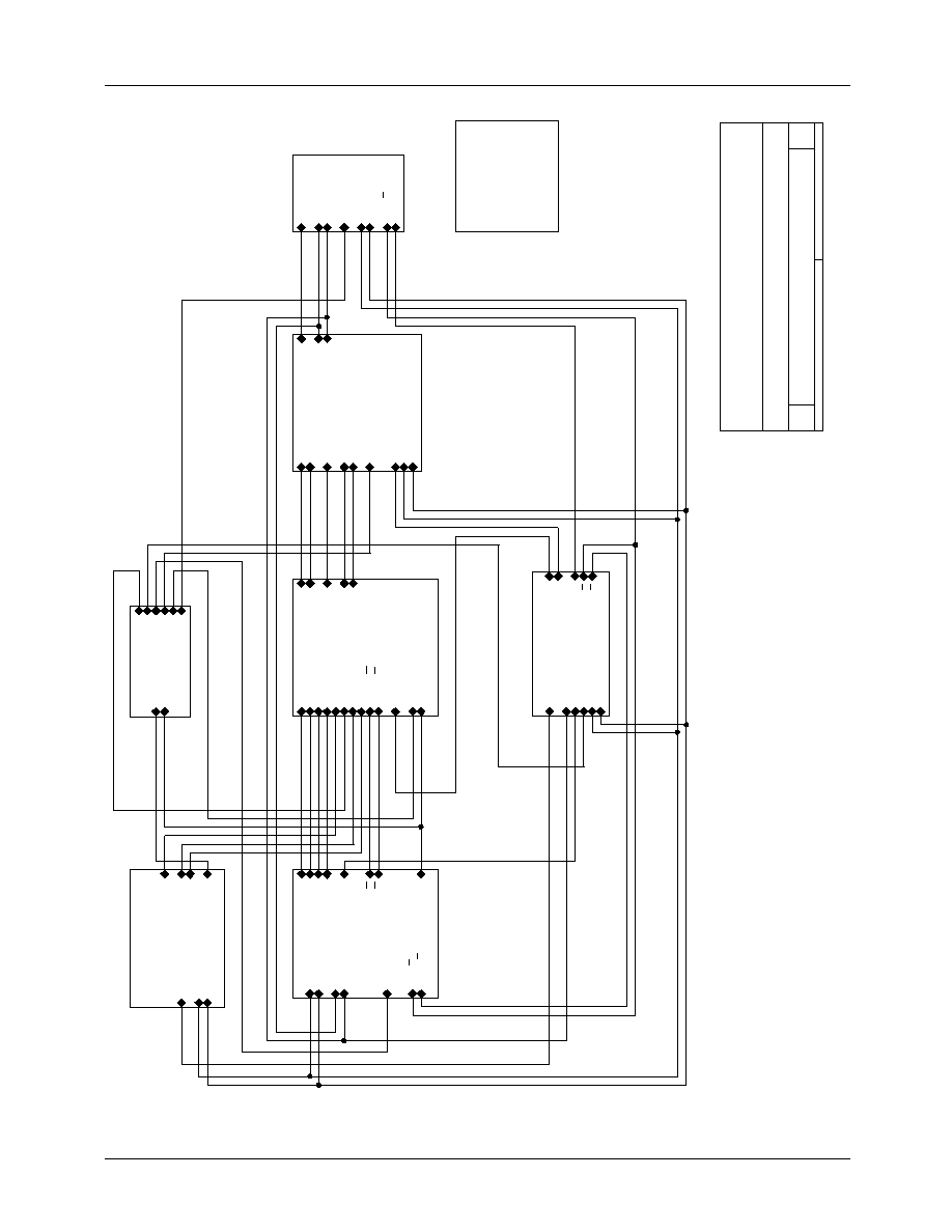
Figure 1.
TMB2193
0.9.0
TO
P
Ra
ytheon Electronics - Semiconductor Division
5580 Morehouse Dr
.
San Diego
, CA 92121
B
11
2
Thursda
y
,
September 04, 1997
Title
Siz
e
Document Number
Re
v
Date:
Sheet
of
CKDRIVE
CKDRIVE
MPXCK
EPXCK
FPXCK
OPXCK
GPXCK
IXPXCK
675MCLK
135MCLK
HEADERIN
HEADERIN
IXHSYNC
IXVSYNC
IXPXCK
MPXCK
SD
A
SCL
HSOUT
VSOUT
PGM_IN
A_DEL[0..9]
B[0..9]
C[0..9]
RESET
FRESET
A[0..9]
FPGA
FPGA
A_DEL[0..9]
B[0..9]
C[0..9]
CVBS[0..7]
GHSYNC
GVSYNC
IXHSYNC
IXVSYNC
PD[0..23]
ECVBS[0..9]
HSIN
VSIN
OLENG[0..5]
FMCU[0..7]
IXPXCK
FPXCK
675MCLK
A[0..9]
GENLOCK
GENLOCK
CVBS[0..7]
SD
A
SCL
GHSYNC
GVSYNC
GPXCK
GMCU[0..6]
MCU
MCU
EMCU[0..3]
GMCU[0..6]
SD
A
PGM_OUT
FMCU[0..7]
PGM_IN
SCL
FRESET
135MCLK
RESET
VSOUT
HEADER
OUT
HEADER
OUT
HSOUT
VSOUT
DCVBS[0..9]
SD
A
SCL
RESET
OPXCK
PGM_OUT
TMC2193
TMC2193
PD[0..23]
ECVBS[0..9]
EPXCK
HSIN
VSIN
DCVBS[0..9]
HSOUT
VSOUT
SD
A
SCL
OLENGI[0..5]
EMCU[0..3]
PO
WER
{Schematic}
A_DEL[0..9]
B[0..9]
C[0..9]
CVBS[0..7]
IXHSYNC\
IXVSYNC\
GHSYNC
GVSYNC
GPXCK
IXPXCK
IXPXCK
FPXCK
MPXCK
PD[0..23]
ECVBS[0..9]
OLENG[0..5]
DCVBS[0..9]
HSIN
OPXCK
GMCU[0..6]
FMCU[0..7]
PGM_IN
RESET\
PGM_OUT
FRESET\
VSIN
HSOUT
SD
A
VSOUT
EMCU[0..3]
EPXCK
SCL
A[0..9]
675MCLK
135MCLK
65-B2193-02