
www.fairchildsemi.com
Features
∑ 8-bit resolution
∑ 50 Msps conversion rate
∑ Low power: 100mW per channel @ 20 Msps
∑ Integral track/hold
∑ Independent Input Clamps
∑ Independent clock inputs
∑ Integral and differential linearity error 0.5 LSB
∑ Differential phase 0.7 degree
∑ Differential gain 1.8%
∑ Single +5V power supply
∑ Three-state TTL/CMOS-compatible outputs
∑ Low cost
Applications
∑ Video digitizing (composite and Y-C)
∑ VGA and CCD digitizing
∑ LCD projection panels
∑ Image scanners
∑ Personal computer video boards
∑ Multimedia systems
∑ Low cost, high speed data conversion
Description
Incorporated into the TMC1103 are three analog-to-digital
(A/D) converters, each with an independent clock, reference
voltage and input clamp. Analog signals are converted to
Triple 8-bit digital words at sample rates up to 50 Msps
(Megasamples per second) per channel.
Integral Track/Hold circuits deliver excellent performance
on signals with full-scale spectral components up to
12 MHz. Innovative two-step conversion architecture and
submicron CMOS technology reduce typical power dissipa-
tion to 100 mW per converter.
Power is derived from a single +5 Volt power supply. Out-
puts are three-state outputs and TTL/CMOS-compatible.
TMC1103 package is a 80-lead Metric Quad Flat Pack
(MQFP). Performance specifications are guaranteed from
0
∞C to 70∞C.
Block Diagram
8-bit
A/D Converter
RTA
DA7-0
OEA
CLKA
VINA
VCLPA
CLPA
RBA
65-1103-01
Clamp
8-bit
A/D Converter
RTB
DA7-0
OEB
CLKB
VINB
VCLPB
CLPB
RBB
Clamp
8-bit
A/D Converter
RTC
DA7-0
OEC
CLKC
VINC
VCLPC
CLPC
RBC
Clamp
TMC1103
Triple Video A/D Converter with Clamps
8-Bit, 50Msps
Rev. 1.2.0
TMC1103
PRODUCT SPECIFICATION
2
Circuit Function
Within the TMC1103 are three 8-bit A/D converters, each
employing two-step architecture to convert an analog input
to a digital output at rates up to 50 Msps. Input signals are
held in integral track/hold stages during the conversion pro-
cess. Operation is pipelined, with one input sample taken and
one output word provided for each CLK
X
cycle.
Each of the three converters function identically. In the fol-
lowing descriptions `X' refers to a generic input/output or
clock where `X' is equivalent to A, B or C.
The first step in the conversion process is a coarse 4-bit
quantization. This determines the range of the subsequent
fine 4-bit quantization step. To eliminate spurious codes, the
fine 4-bit A/D quantizer output is gray-coded and converted
to binary before it is combined with the coarse result to form
a complete 8-bit result.
Analog Input and Voltage References
Each A/D accepts analog signals in the range R
BX
to R
TX
into
digital data. Input signals outside this range produce "satu-
rated" 00h or FFh output codes. The device will not
be damaged by signals within the range A
GND
to V
DDA
.
Input range is very flexible and extends from the +5 Volt
power supply to ground. Nominal input range is 2 Volts,
extending from 0.6V to 2.6V. Characterization and
performance is specified over this range. However, the
part will function with a full-scale range from 1.0V to 5.0V.
A smaller input range may simplify analog signal condition-
ing circuitry, at the expense of additional noise sensitivity
and some reduced differential linearity performance.
External voltage reference sources are connected to the R
TX
and R
BX
pins. R
BX
can be grounded. Within each A/D con-
verter is a reference resistor ladder comprising 255 resistors
that are accessed by the TMC1103 comparators. R
TX
is con-
nected to the top of the ladder, R
BX
to the bottom. Gain and
offset errors are directly related to the accuracy and stability
of the applied reference voltages.
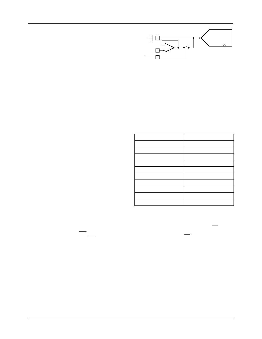
Input Clamps
A clamp circuit is connected to the input pin V
INX
of each of
the three A/D converters. With CLP
X
LOW, the input pin is
clamped to the voltage at V
CLPX
. If CLP
X
is HIGH, the
input pin is high impedance. Clamping adds an offset voltage
to an AC coupled signal to adjust this signal's amplitude to
the A/D converter input voltage range.
The analog input is corrected through a 0.1
mF capacitor to
V
INX
. The source impedance of the analog source should be
less than 50 Ohms. Current pulses through the capacitor over
several clamp cycles until the voltage across the capacitor
equals the difference between V
CLPX
and the voltage at the
analog source during the clamping period. When the switch
is open, the voltage on the coupling capacitor is added to the
analog input, producing a a DC offset input signal.
Input Clamp Circuit
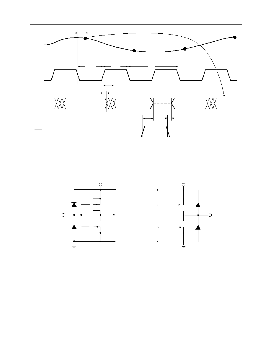
Digital Inputs and Outputs
Sampling of the applied input signal occurs on the falling
edge of the CLK
X
signal (Figure 1). Output data is delayed
by 2 1/2 CLK
X
cycles and is valid following the rising edge
of CLK
X
. Previous output data remains valid for t
HO
(Out-
put Hold Time). New data becomes valid t
D
(Output Delay
Time) after this rising edge of CLK
X
.
Whenever the analog input signal is sampled and found to be
at a level beyond the A/D conversion range, the output limits
at 00h or FFh, as appropriate.
Table 1. A/D Output Coding
Note: 1 LSB = (R
TX
≠ R
BX
) / 255
The outputs of the TMC1103 are CMOS- and
TTL-compatible, and are capable of driving four low-power
Schottky TTL loads. An Output Enable control, OE
X
, places
the A/D outputs in a high-impedance state when HIGH.
The outputs are enabled when OE
X
is LOW.
Power and Ground
The TMC1103 operates from a single +5 Volt power supply.
For optimum performance, an analog ground plane should
be placed under the TMC1103 the A
GND
and D
GND
pins
should be connected to the system analog ground plane.
Input Voltage
Output
R
TX
+ 1 LSB
FF
R
TX
FF
R
TX
- 1 LSB
FE
∑ ∑ ∑
∑ ∑ ∑
R
BX
+ 128 LSB
80
R
BX
+ 127 LSB
7F
∑ ∑ ∑
∑ ∑ ∑
R
BX
+ 1 LSB
01
R
BX
00
R
BX
- 1 LSB
00
A/D Converter
Analog
Input
V
INX
0.1
µ
F
V
CLPX
CLP
X
65-1103-02
PRODUCT SPECIFICATION
TMC1103
3
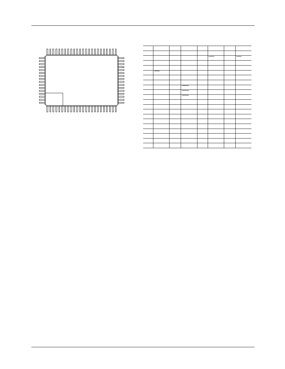
Pin Assignments
NC
DA
5
DA
6
DA
7
OE
A
V
DD
V
DD
NC
CLK
A
NC
V
DDA
V
INA
AGND
R
TA
R
BA
V
CLPA
V
CLPB
V
CLPC
DGND
DGND
1
2
3
4
5
6
7
8
9
10
11
12
13
14
15
16
17
18
19
20
DGND
DGND
NC
NC
DGND
DGND
V
DD
CLP
A
CLP
B
CLP
C
NC
DGND
DGND
DC
0
DC
1
DC
2
DC
3
DC
4
DC
5
DC
6
21
22
23
24
25
26
27
28
29
30
31
32
33
34
35
36
37
38
39
40
Pin
Name
Pin
Name
DC
7
OE
C
V
DD
V
DD
CLK
C
NC
V
DDA
V
INC
AGND
R
TC
R
BC
R
BB
R
TB
AGND
V
INB
V
DDA
NC
CLK
B
NC
V
DD
41
42
43
44
45
46
47
48
49
50
51
52
53
54
55
56
57
58
59
60
V
DD
OE
B
DB
7
DB
6
DB
5
DB
4
DB
3
DB
2
DB
1
DB
0
DGND
DGND
NC
DGND
DGND
DA
0
DA
1
DA
2
DA
3
DA
4
61
62
63
64
65
66
67
68
69
70
71
72
73
74
75
76
77
78
79
80
Pin
Name
Pin
Name
1
24
65-1103-03
25
40
41
64
65
80

PRODUCT SPECIFICATION
TMC1103
4
Pin Descriptions
Pin Name
Pin Number
Value
Pin Function Description
A/D Converters
V
INA
, V
INB
,
V
INC
12, 55, 48
R
TX
to
R
BX
Analog Inputs. The input voltage conversion range lies between the
voltage applied to the R
TX
and R
BX
pins.
R
TA
, R
TB
, R
TC
14, 53, 50
2.6V
Reference Voltage, Top Inputs. DC voltages applied to R
TA
, R
TB
and R
TC
define highest value of V
INX
.
R
BA
, R
BB
, R
BC
15, 52, 51
0.6V
Reference Voltage, Bottom Inputs. DC voltages applied to R
BA
,
R
BB
and R
BC
define lowest value of V
INX
.
CLK
A
, CLK
B
,
CLK
C
9, 58, 45
CMOS
Clock Inputs. CMOS-compatible. V
INX
is sampled on the falling
edge of CLK
X
.
DA
7-0
4, 3, 2, 80, 79,
78, 77, 76
CMOS/
TTL
Data outputs, Converter A (D
7
= MSB). Eight-bit CMOS- and
TTL-compatible digital outputs. Valid data is output on the rising
edge of CLK
X
.
DB
7-0
63, 64, 65, 66,
67, 68, 69, 70
CMOS/
TTL
Data outputs, Converter B (D
7
= MSB). Eight-bit CMOS- and
TTL-compatible digital outputs. Valid data is output on the rising
edge of CLK
X
.
DC
7-0
41, 40, 39, 38,
37, 36, 35, 34
CMOS/
TTL
Data outputs, Converter C (D
7
= MSB). Eight-bit CMOS- and
TTL-compatible digital outputs. Valid data is output on the rising
edge of CLK
X
.
OE
A
, OE
B
, OE
C
5, 62, 42
CMOS
Output Enable Inputs. CMOS-compatible. When LOW, the A/D
output is enabled. When HIGH, the output is in a high-impedance
state.
Clamps
V
CLPA
, V
CLPB
,
V
CLPB
16, 17, 18
R
TX
to
R
BX
Clamp Reference Voltage. One reference for each clamp. A V
INX
input is clamped to V
CLPX
when CLP
X
is low.
CLP
A
, CLP
B
,
CLP
C
28, 29, 30
CMOS
Clamp Pulse Inputs. One input for each A/D clamp. When CLP
X
is
low, the V
INX
input is clamped to the V
CLPX
clamp voltage.
Power
V
DDA
11, 47, 56
+5V
Analog Supply Voltage. +5 Volt power inputs. These should come
from the same power source and be decoupled to A
GND
.
V
DD
6, 7, 27, 28, 29,
30, 43, 44, 60,
61
+5V
Digital Supply Voltage. +5 Volt power inputs. These should come
from the same power source and be decoupled to A
GND
.
A
GND
13, 49, 54
0.0V
Analog Ground. Ground connections. These pins should be
connected to the system analog ground plane.
D
GND
16, 17, 18, 19,
20, 21, 22, 25,
26, 32, 33, 71,
72, 74, 75
0.0V
Digital Ground. Ground connections. These pins should be
connected to the system analog ground plane.
No Connect
N/C
1, 8, 10, 23, 24,
31, 46, 57, 59,
73
open
Not Connected.
PRODUCT SPECIFICATION
TMC1103
5
Figure 1. Timing
Equivalent Circuits and Threshold Levels
Figure 2. Equivalent Digital Input Circuit
Figure 3. Equivalent Digital Output Circuit
VINX
Sample N
Sample N+1
Data N-3
Data N-2
Data N-1
Data N
Hi-Z
Sample N+2
Sample N+3
tSTD
tPWL
tPWH
tDIS
tENA
tDO
tHO
1/fS
CLKX
65-1103-04
DX7-0
OEX
Digital
Input
V
DD
p
n
27014B
GND
V
DD
p
n
27011B
GND
Digital
Output