TMC1175A Video A/D Converter
TMC1175A
Video A/D Converter
8 bit, 40 Msps
www.fairchildsemi.com
REV. 1.3.3 2/28/02
Features
· 8-Bit resolution
· 40 Msps conversion rate
· Low power: 100mW at 20 Msps
· Integral track/hold
· Integral and differential linearity error 0.5 LSB
· Single or dual +5 Volt supplies
· Differential phase 0.5 degree
· Differential gain 1.5%
· Three-state TTL/CMOS-compatible outputs
· Low cost
Applications
· Video digitizing
· VGA and CCD digitizing
· LCD projection panels
· Image scanners
· Personal computer video boards
· Multimedia systems
· Low cost, high speed data conversion
Description
The TMC1175A analog-to-digital (A/D) converter employs
a two-step flash architecture to convert analog signals into
8-bit digital words at sample rates of up to 40 Msps
(Megasamples per second). An integral Track/Hold circuit
delivers excellent performance on signals with full-scale fre-
quency components up to 12 MHz. Innovative architecture
and submicron CMOS technology limit typical power dissi-
pation to 100 mW.
Power may be derived from either single or dual +5V
supplies. Internal voltage reference resistors allow self-bias
operation. Input capacitance is very low, simplifying or
eliminating input driving amplifiers. All digital three-state
outputs are TTL- and CMOS-compatible.
The TMC1175A is available in 24-lead plastic SOIC, and
28-lead J-lead PLCC packages. Performance specifications
are guaranteed from -20°C to 75°C.
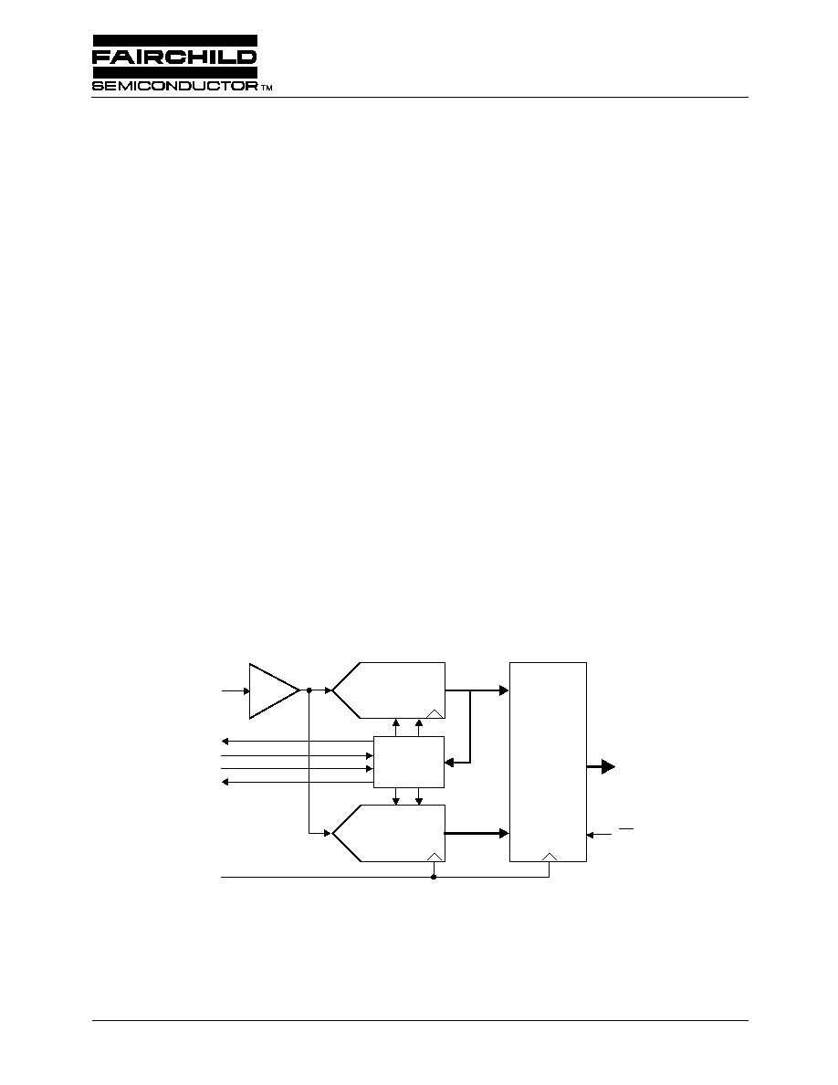
Block Diagram
Reference
Matrix
D
7-0
V
IN
VR+
R
T
R
B
VR
Track/
Hold
OE
CONV
24453A
Coarse
Quantizer
Digital
Error-
Corrector
Fine
Quantizer
TMC1175A
PRODUCT SPECIFICATION
2
REV. 1.3.3 2/28/02
Functional Description
The TMC1175A 8-bit A/D converter uses a two-step archi-
tecture to perform analog-to-digital conversion at rates up to
40 Msps. The input signal is held in an integral track/hold
stage during the conversion process. Operation is pipelined,
with one input sample taken and one output word provided
for each CONVert cycle.
The first step in the conversion process is a coarse 4-bit
quantization. This determines the range of the subsequent
fine 4-bit quantization step. To eliminate spurious codes, the
fine 4-bit A/D quantizer output is gray-coded and converted
to binary before it is combined with the coarse result to form
a complete 8-bit result.
Analog Input and Voltage References
The TMC1175A converts analog signals in the range R
B
to
R
T
into digital data. Input signals outside that range produce
"saturated" 00h or FFh output codes. The device will not be
damaged by signals within the range A
GND
to V
DDA
.
Input voltage range is very flexible and extends from the +5
Volt power supply to ground. Performance is specified over
the optimom 2 volt input range: 0.6V to 2.6V. However, the
part will function with a full-scale range from 1.0V to 5.0V.
A reduced input range may simplify analog signal condition-
ing circuitry, at the expense of additional noise sensitivity
and reduced differential linearity. Increasing the range can
improve differential linearity, but imposes a greater burden
on the input signal conditioning circuitry.
In many applications, external voltage reference sources are
connected to the R
T
and R
B
pins. R
B
can be grounded. Gain
and offset errors are directly related to the accuracy and sta-
bility of the applied reference voltages.
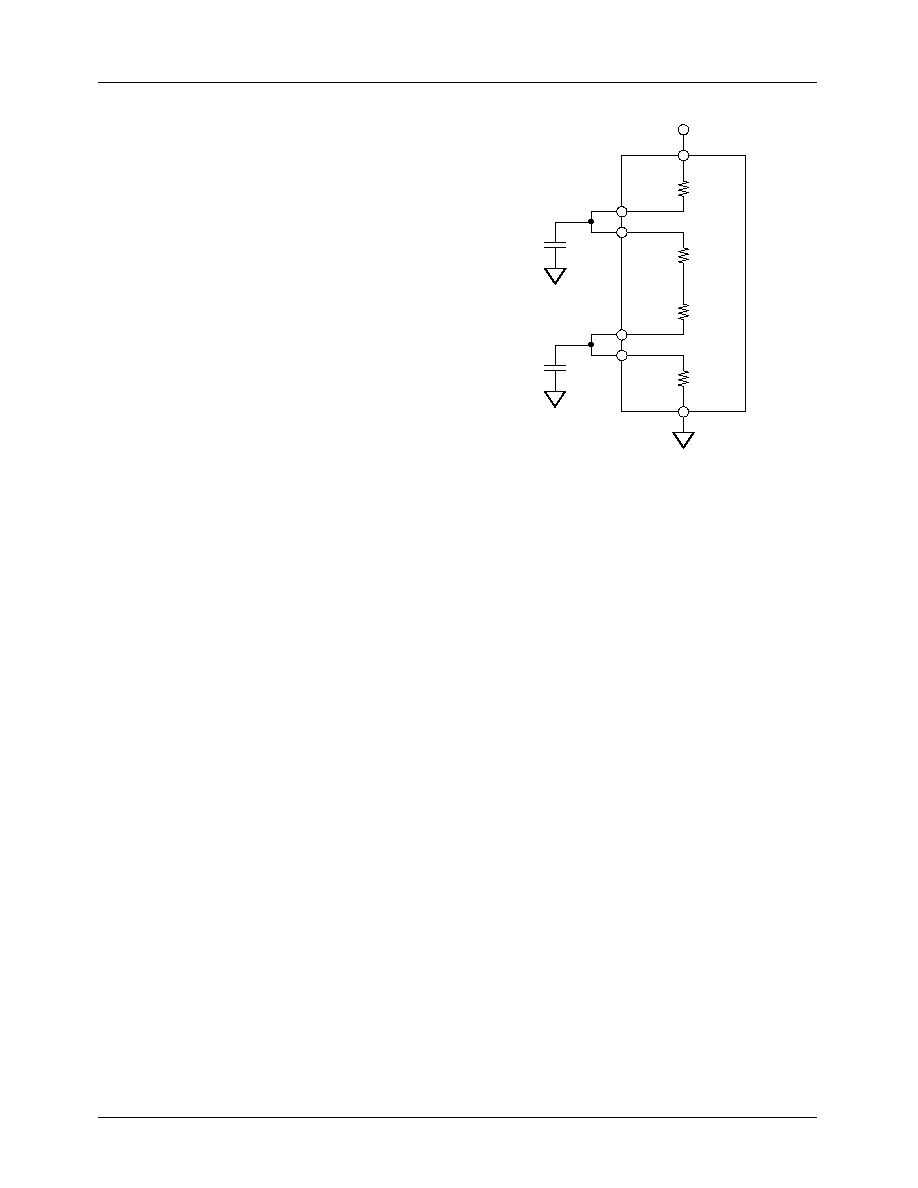
Two reference pull-up and pull-down resistors connected to
VR+ and VR are provided internally for operation without
external voltage reference circuitry (Figure 1). The reference
voltages applied to R
T
and R
B
may be generated by connect-
ing VR+ to R
T
and VR- to R
B
. The power supply voltage is
divided by the on-chip resistors to bias the R
T
and R
B
points.
This sets-up the converter for operation in its nominal range
from 0.6V to 2.6V.
Figure 1. Reference Resistors
With V
DDA
at 5.0V, connecting VR+ to R
T
and grounding
R
B
will provide an input range from 0.0V to 2.27V, while
connecting R
T
to V
DDA
and R
B
to VR- produces a full scale
range of 3.85V referenced to V
DDA
. External resistors may
also be employed to provide arbitrary reference voltages, but
they will not match the temperature coefficient of the on-
chip resistors as well as R+ and R-, and will cause the con-
verter transfer function to vary with temperature.
With this implementation, errors in the power supply voltage
end up on the conversion data output.
Because a two-step conversion process is employed, it is
important that the references remain stable during the
ENTIRE conversion process (two clock cycles). The refer-
ence voltage can then be changed, but any conversion in
progress during a reference change is invalid.
VDDA
VR+
R
T
R+
324
RREF
270
R
81
R
B
VR
+2.6V
+0.6V
27010A
PRODUCT SPECIFICATION
TMC1175A
REV. 1.3.3 2/28/02
3
Table 1. Output Coding
Note:
1. LSB = (R
T
R
B
) / 255
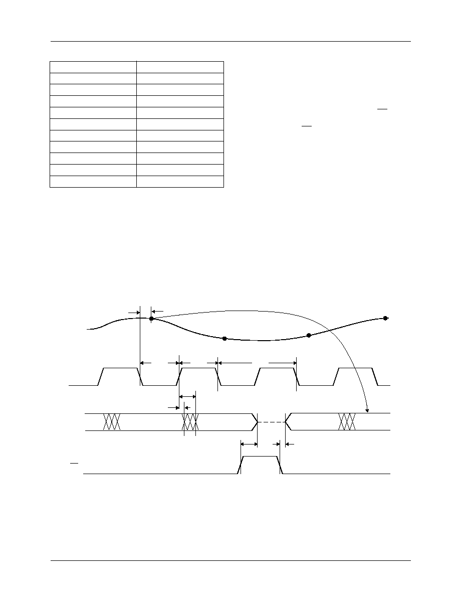
Digital Inputs and Outputs
Sampling of the applied input signal takes place on the fall-
ing edge of the CONV signal (Figure 2). The output word is
delayed by 2 1/2 CONV cycles. It is then available after the
rising edge of CONV. The previous data on the output
Input Voltage
Output
R
T
+ 1 LSB
FF
R
T
FF
R
T
1 LSB
FE
· · ·
· · ·
R
B
+ 128 LSB
80
R
B
+ 127 LSB
7F
· · ·
· · ·
R
B
+ 1 LSB
01
R
B
00
R
B
1 LSB
00
remain valid for t
HO
(Output Hold Time), satisfying any
hold time requirement of the receiving circuit. The new data
become valid t
DO
(Output Delay Time) after this rising edge
of CONV.
The outputs of the TMC1175A are CMOS- and TTL-com-
patible, and are capable of driving four low-power Schottky
TTL (54/74LS) loads. An Output Enable control, OE, places
the outputs in a high-impedance state when HIGH. The out-
puts are enabled when OE is LOW.
Power and Ground
To minimize noise injection into the analog section, V
DDA
may be connected to a separate regulated +5 volt supply.
V
DDD
may be connected to a digital supply. Power up
sequence is immaterial. Latch-up will not occur.
A
GND
and D
GND
pins should be connected to a common
ground plane. For optimum performance treat analog and
digital PWB traces as transmission lines. Route analog
connections cleanly to the TMC1175A. Segregate digital
connections and if necessary terminate clocks to eliminate
ringing. Prevent digital returm currents from flowing across
analog input sections of the TMC1175A.
Figure 2. Conversion Timing
CONV
D
7-0
ORP
ORN
OE
V
IN
24455A
Data N3
Data N2
Data N1
Data N
t
STO
t
PWL
t
HO
t
DIS
t
ENA
t
DO
t
PWH
1/f
S
Hi-Z
Sample N
Sample N+1
Sample N+2
Sample N+3
TMC1175A
PRODUCT SPECIFICATION
4
REV. 1.3.3 2/28/02
Analog input
External Clock
Upper comparators block
Lower comparators A block
Upper data
Lower reference voltage
Lower data A
Lower comparators B block
Lower data B
Digital output
S (1)
S (1)
H (1)
C (1)
S (2)
C (2)
C (3)
H (3)
C (3)
S (3)
S (3)
S (4)
C (4)
C (1)
MD (0)
MD (1)
MD (2)
MD (3)
RV (0)
RV (1)
RV (2)
RV (3)
LD (-1)
LD (1)
LD(-2)
LD(0)
LD(2)
Out(-2)
Out(-1)
Out(0)
Out(1)
V(1)
V(2)
V(3)
V(4)
H (0)
C (0)
S (2)
H (2)
C (2)
S (4)
H (94)
65-7568
Figure 3. Internal Timing
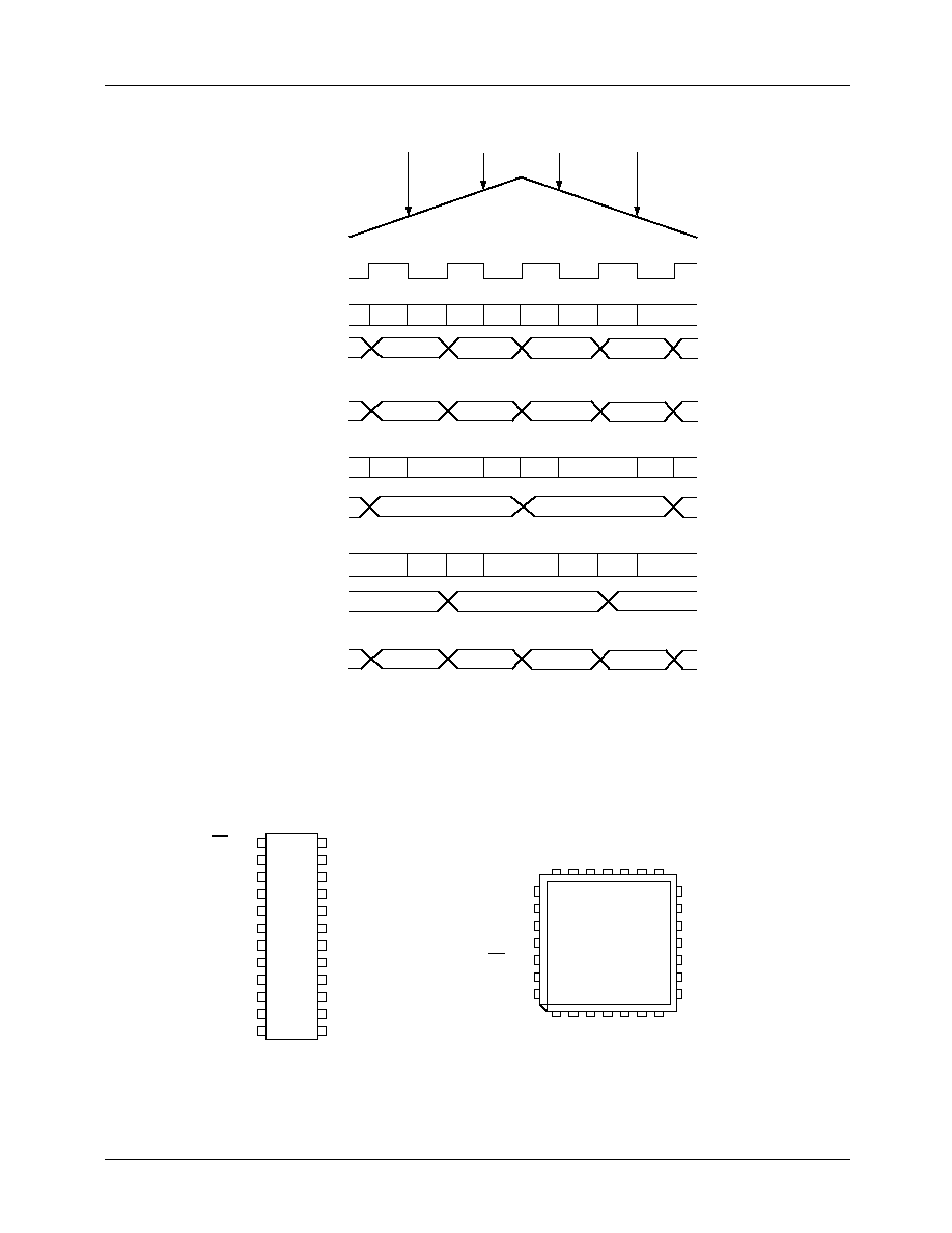
Pin Assignments
27
R
B
1
2
3
4
5
6
7
8
9
10
11
12
24
23
22
21
20
19
18
17
16
15
14
13
M7 Package
24454A
N/C
D
7
V
DDD
V
DDD
R3 Package
D1
D2
D3
N/C
N/C
D4
D5
D6
CONV
A
GND
A
GND
V
IN
V
DDA
R
T
VR+
V
DDA
V
DDA
1
N/C
26
2
3
28
4
5
6
7
8
9
10
11
12
24
25
23
22
21
20
19
18
17
16
15
14
13
VR
D
GND
D
GND
D
GND
R
B
VR
A
GND
A
GND
V
IN
V
DDA
R
T
VR+
V
DDA
V
DDA
V
DDD
OE
OE
D
GND
D
0
D
0
D
1
D
2
D
3
D
4
D
5
D
6
D
7
V
DDD
CONV

PRODUCT SPECIFICATION
TMC1175A
REV. 1.3.3 2/28/02
5
Pin Descriptions
Pin Name
Pin Number
Pin Type Pin Function Description
M7
R3
Inputs
V
IN
19
23
R
T
R
B
Analog Input. The input voltage conversion range lies between the
voltages applied to the RT and RB pins.
R
T
17
20
2.6V
Reference Voltage Top Input. R
T
is the top input to the reference
resistor ladder. A DC voltage applied to R
T
defines the positive end
of the V
IN
conversion range.
R
B
23
27
0.6V
Reference Voltage Bottom Input. R
B
is the bottom input to the
reference resistor ladder. A DC voltage applied to R
B
defines the
negative end of the V
IN
conversion range.
VR+
16
19
Reference Voltage Top Source. VR+ is the internal pull-up
reference resistor for self-bias operations.
VR
22
26
Reference Voltage Bottom Source. VR- is the internal pull-down
reference resistor for self-bias operations.
OE
1
2
CMOS
Output Enable. (CMOS-compatible) When LOW, D
7-0
are enabled.
When HIGH, D
7-0
are in a high-impedance state.
CONV
12
14
CMOS
Convert (Clock) Input. (CMOS-compatible) V
IN
is sampled on the
falling edge of CONV.
Outputs
D
7-0
103
129,
74
CMOS/
TTL
Data Outputs (D7 = MSB). Eight-bit CMOS- and TTL-compatible
digital outputs. Data is output following the rising edge of CONV.
Power
V
DDA
14, 15, 18
17, 18,
21
+5V
Analog Supply Voltage. Independent +5 volt power connection to
analog comparator circuits.
V
DDD
11, 13
13, 16
+5V
Digital Supply Voltage. Independent +5 volt power connection to
digital error correction and output drivers.
A
GND
20, 21
24, 25
0.0V
Analog Ground. Connect to the system analog ground plane.
D
GND
2, 24
3, 28
0.0V
Digital Ground. Connect to the system analog ground plane.
No Connect
N/C
1, 8, 15,
22
open
Not Connected.
Bandwidth Specification Notes
The specification for bandwidth of an A/D converter is some-
what different from the normal frequency-response specifi-
cation used in amplifiers and filters. An understanding of the
differences will help in selecting converters properly for par-
ticular applications.
A/D conversion comprises two distinct processes: sampling
and quantizing. Sampling is "grabbing" a snapshot of the
input signal and holding it steady for quantizing. The quan-
tizing process is approximating the analog input, which may
be any value within the conversion range, with its nearest
numerical value. While sampling is a high-frequency pro-
cess, quantizing operates on a dc signal, held steady by the
track/hold circuit. Therefore, the sampling process is what
relates to the dynamic characteristics of the converter.
Sampling involves an aperture time, the time during which
the track/hold is trying to capture the input signal and settle
on a dc value to hold. It is analogous to the shutter speed of a
camera: the shorter the aperture (or faster the shutter) the less
the signal will be blurred, and the less uncertainty there will
be in the quantized value.
For example, a 10 MHz sinewave with a 1V peak amplitude
(2Vp-p) has a maximum slew rate of 2
fA at zero crossing,
or 62.8V/µs. With an 8-bit A/D converter, q (the quantization
step size) = 2V/255 = 7.8mV. The input signal will slew one
LSB in 124ps. To limit the error (and noise) contribution due
to aperture effects to 1/2LSB, the aperture must be shorter
than 62ps.