
www.fairchildsemi.com
Features
∑ Low power CMOS
∑ TMC2011A is a pin compatible replacement for the
TDC1011 and TMC2011
∑ TMC2211A is a pin compatible replacement for the
TMC2111
∑ Inputs and outputs are TTL compatible
∑ DC≠40MHz clock rate
∑ Selectable delay lengths (TMC2011A: 3 to 18 stages,
TMC2111A: 1 to 16 stages)
∑ Special 4-bit wide mixed-delay mode (TMC2011A)
∑ Available in 24-pin CERDIP and plastic DIP and 28-lead
Plastic Leadless Chip Carrier
Applications
∑ Video filtering
∑ High speed data registers
∑ Local storage registers
∑ Digital delay lines
∑ Television special effects
∑ Pipeline register
Description
The TMC2011A and TMC2111A are high-speed, byte-wide
shift registers with programmable delay lengths.
The TMC2011A can be programmed to any length between
3 and 18 stages. It offers a special split-word mode which
allows for mixed delay lengths. The TMC2011A, con-
structed in low-power CMOS, is pin and function compatible
with the bipolar TDC1011.
The TMC2111A is a byte-wide shift register that can be pro-
grammed to lengths of 1 to 16 stages.
The TMC2011A and TMC2111A are fully synchronous,
with all operations controlled by a single master clock. Input
and output registers are positive-edge triggered D-type flip-
flops. The length and mode controls are also registered. Both
devices operate with a maximum clock rate of 40 MHz.
Fabricated in a submicron CMOS process, the TMC2011A
and TMC2111A are TTL-compatible, and are available in
24-pin CERDIP and Plastic DIP packages as well as a
28-lead Plastic Leadless Chip Carrier.
Block Diagrams
TMC2011A
TMC2111A
R
1
DI
3-0
DO
3-0
DO
7-4
L
3-0
DI
7-4
MC
CLK
4
4
4
4-Bit Wide
1 of 16 Selector
4-Bit Wide
1 of 16 Selector
4
4
65-2011A-01
4
4
4
4
4
4
4
4
4
4
4
4
4
4
R
2
R
3
R
16
R
17
R
L
R
I
R
1
R
2
R
3
R
16
R
17
R
18
R
18
8
8
8
8
8
R
1
R
14
R
15
DO
7-0
L
3-0
DI
7-0
4
4
8-Bit Wide
1 of 16 Selector
8
8
65-2011A-02
8
R
L
R
16
CLK
TMC2011A/2111A
Variable-Length Shift Register
Rev. 1.1.0

TMC2011A/2111A
PRODUCT SPECIFICATION
2
Functional Description
The TMC2011A consists of two 4-bit wide, programmable
length shift registers. The TMC2111A consists of a single
8-bit wide, programmable length shift register. The internal
registers of each device share control signals and a common
clock.
Pin Assignments
24 Lead DIP (B2, N2) Packages
28 Lead PLCC (R3) Package
DI
0
TMC2011A
1
12
24
65-2011A-03
13
DI
1
DI
2
DI
3
L
0
L
1
V
DD
CLK
DI
4
DI
5
DI
6
DI
7
DO
0
DO
1
DO
2
DO
3
L
2
L
3
GND
MC
DO
4
DO
5
DO
6
DO
7
DI
0
TMC2111A
1
12
24
13
DI
1
DI
2
DI
3
L
0
L
1
V
DD
CLK
DI
4
DI
5
DI
6
DI
7
DO
0
DO
1
DO
2
DO
3
L
2
L
3
GND
GND
DO
4
DO
5
DO
6
DO
7
DI
3
L
0
L
1
V
DD
CLK
DI
4
NC
NC
L
2
L
3
GND
GND
MC
NC
DI
2
DI
1
DI
0
DO
0
DO
1
DO
2
DO
3
DI
5
DI
6
DI
7
DO
7
DO
6
DO
5
DO
4
TMC2011A
1 28
65-2011A-04
DI
3
L
0
L
1
V
DD
CLK
DI
4
NC
NC
L
2
L
3
GND
GND
MC
NC
DI
2
DI
1
DI
0
DO
0
DO
1
DO
2
DO
3
DI
5
DI
6
DI
7
DO
7
DO
6
DO
5
DO
4
TMC2111A
1 28

PRODUCT SPECIFICATION
TMC2011A/2111A
3
Pin Descriptions ≠ TMC2011A
Pin Name
Pin Number
Pin Function Description
DIP
PLCC
Power
V
DD
7
8
Supply Voltage.
The TMC2011A and operates from a single +5V supply.
All power and ground lines must be connected.
GND
18
21,22
Ground.
The TMC2011A operates from a single +5V supply. All power
and ground lines must be connected.
Data Inputs
DI
7-0
12,11,10,
9,4,3,2,1
14,13,12,
10,5,4,3,2
Data Input.
Eight inputs are provided for the data, which pass through the
shift register unchanged. The eight inputs on the TMC2011A are divided
into two groups of four bits to allow mixed delay operation. The lengths of
these two groups are different when the Mode Control (MC) is HIGH (see
Table 1). When MC is LOW both groups have equal delays.
Data Outputs
DO
7-0
13,14,15,
16,21,22,
23,24
15,16,17,
18,26,27,
28,1
Data Output.
The outputs of the shift register are delayed relative to the
input signals. The amount of the delay is programmable (see Table 1).
The outputs remain valid for a minimum of t
HO
nanoseconds after the
leading edge of CLK. This allow the data to be latched into circuits with
non-zero hold time requirements.
Controls
CLK
8
9
Master Clock.
All inputs and outputs are synchronous and operate from a
single master clock. All operations occur on the rising edge of the master
clock.
L
3-0
19,20,6,5
23,24,7,6
Length Select.
The length select input is used to determine the register
delay of the TMC2011A. This input is registered and affects the output t
DO
after the clock edge after it is input to the device (see Timing Diagram).
Delay lengths are specified in Table 1.
MC
17
20
Mode Control.
The Mode Control is used to select the special 4-bit wide
split mode. When HIGH, the delay on DO
7-4
is fixed at 18 stages, while
DO
3-0
have the delay specified by the length select. When MC is LOW, all
eight bits have equal delays as specified by the length select.
TMC2011A/2111A
PRODUCT SPECIFICATION
4
Table 1. Programming Length Controls
Pin Descriptions ≠ TMC2111A
Pin Name
Pin Number
Pin Function Description
DIP
PLCC
Power
V
DD
7
8
Supply Voltage.
The TMC2111A operates from a single +5V supply. All
power and ground lines must be connected.
GND
17,18
20,21,22
Ground.
The TMC2111A operates from a single +5V supply. All power
and ground lines must be connected.
Data Inputs
DI
7-0
12,11,10,
9,4,3,2,1
14,13,12,
10,5,4,3,2
Data Input.
Eight inputs are provided for the data, which pass through the
shift register unchanged. The TMC2111A consists of a single group of
eight bits with all data bits having equal delays.
Data Outputs
DO
7-0
13,14,15,
16,21,22,
23,24
15,16,17,
18,26,27,
28,1
Data Output.
The outputs of the shift register are delayed relative to the
input signals. The amount of the delay is programmable (see Table 1).
The outputs remain valid for a minimum of t
HO
nanoseconds after the
leading edge of CLK. This allow the data to be latched into circuits with
non-zero hold time requirements.
Controls
CLK
8
9
Master Clock.
All inputs and outputs are synchronous and operate from a
single master clock. All operations occur on the rising edge of the master
clock.
L
3-0
19,20,6,5
23,24,7,6
Length Select.
The length select input is used to determine the register
delay of the TMC2111A. This input is registered and affects the output t
DO
after the clock edge after it is input to the device (see Timing Diagram).
Delay lengths are specified in Table 1.
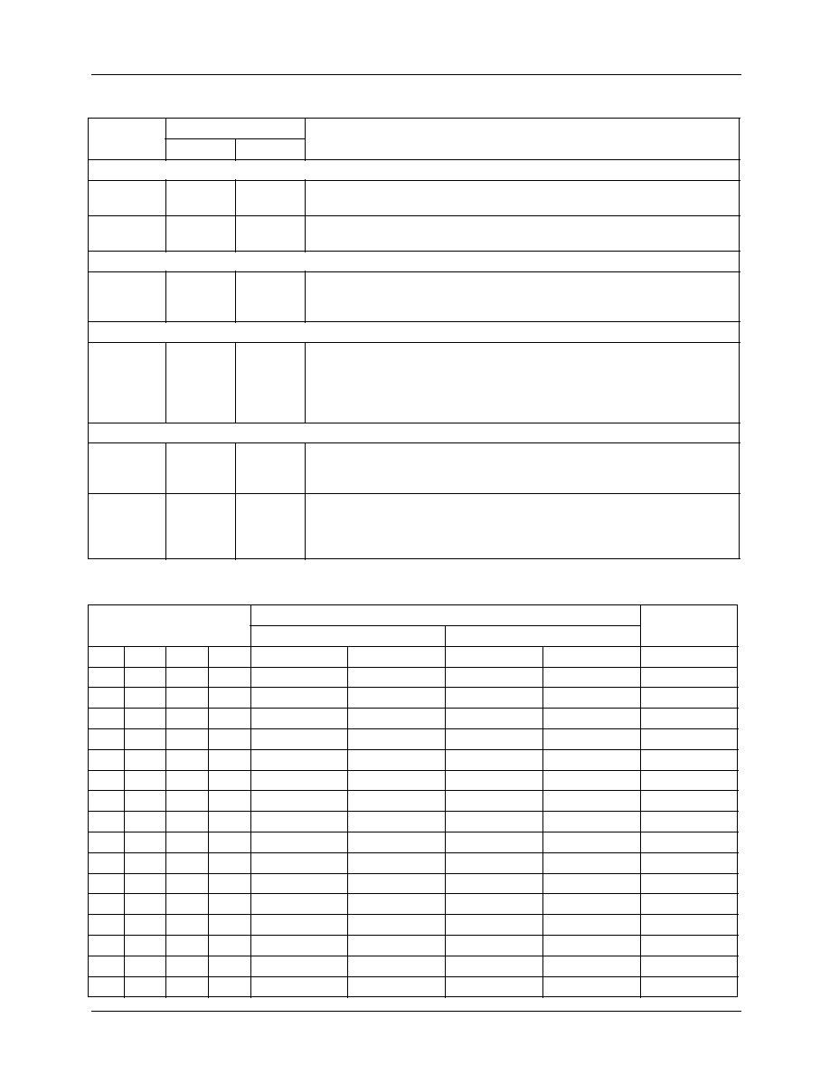
TMC2011A
TMC2111A
Input Code
Mode (MC) =0
Mode (MC) =1
L
3
L
2
L
1
L
0
DO
3-0
Length
DO
7-4
Length
DO
3-0
Length
DO
7-4
Length
DO
7-0
Length
0
0
0
0
3
3
3
18
1
0
0
0
1
4
4
4
18
2
0
0
1
0
5
5
5
18
3
0
0
1
1
6
6
6
18
4
0
1
0
0
7
7
7
18
5
0
1
0
1
8
8
8
18
6
0
1
1
0
9
9
9
18
7
0
1
1
1
10
10
10
18
8
1
0
0
0
11
11
11
18
9
1
0
0
1
12
12
12
18
10
1
0
1
0
13
13
13
18
11
1
0
1
1
14
14
14
18
12
1
1
0
0
15
15
15
18
13
1
1
0
1
16
16
16
18
14
1
1
1
0
17
17
17
18
15
1
1
1
1
18
18
18
18
16

PRODUCT SPECIFICATION
TMC2011A/2111A
5
Absolute Maximum Ratings
(beyond which the device may be damaged)
1
Notes:
1. Functional operation under any of these conditions is NOT implied. Performance and reliability are guaranteed only if
Operating Conditions are not exceeded.
2. Applied voltage must be current limited to specified range.
3. Forcing voltage must be limited to specified range.
4. Current is specified as conventional current flowing into the device.
Operating Conditions
Parameter
Min
Typ
Max
Unit
Supply Voltage
-0.5
7.0
V
Input Voltage
-0.5
V
DD
+ 0.5
V
Output, Applied Voltage
2
-0.5
V
DD
+ 0.5
V
Output, Externally Forced Current
3,4
-3.0
6.0
mA
Output, Short Circuit Duration (single output in HIGH state to
ground)
1
sec
Operating, Ambient Temperature
-20
110
∞
C
Junction Temperature
140
∞
C
Storage Temperature
-65
150
∞
C
Lead Soldering (10 seconds)
300
∞
C
Parameter
Min
Nom
Max
Units
V
DD
Power Supply Voltage
4.75
5.0
5.25
V
f
CLK
Clock frequency
TMC2011A, 2111A
30
MHz
TMC2011A-1, 2111A-1
40
t
PWH
CLK pulse width, HIGH
12
ns
t
PWL
CLK pulse width, LOW
12
ns
t
S
Input Data Set-up Time
6
ns
t
H
Input Data Hold Time
1
ns
V
IH
Input Voltage, Logic HIGH
DI
7-0
, L
3-0
, MC
2.0
V
CLK
2.6
V
IL
Input Voltage, Logic LOW
0.8
V
I
OH
Output Current, Logic HIGH
-2.0
mA
I
OL
Output Current, Logic LOW
4.0
mA
T
A
Ambient Temperature, Still Air
0
70
∞
C