Äîêóìåíòàöèÿ è îïèñàíèÿ www.docs.chipfind.ru
www.fairchildsemi.com
REV. 1.0.4 6/19/01
Features
· Fully integrated acquisition
· 3-channel video input multiplexer
· Two-stage (analog and digital) video clamp
· Automatic gain adjustment
· Sync detection and separation
· Pixel and subpixel adjustment of video-to-sync output
timing
· Genlock to any NTSC or PAL format, including PAL-M
and PAL-N
· Pixel clock generation
· 8-bit video A/D conversion
· Standard R-bus serial microprocessor interface
· User-selectable line-locked pixel rates include:
12.27 MHz NTSC & PAL-M
13.5 MHz
NTSC & all PAL
14.75 MHz PAL (non-M) TMC2072-1 only
15.0 MHz
PAL (non-M) TMC2072-1 only
· Direct interface to Fairchild Semiconductor video
encoders and decoders
· Built-in circuitry for crystal oscillator
· No tuning or external voltage reference required
· Space-saving 100-lead MQFP package
Applications
· Frame grabber
· Digital videotape recorders
· Desktop video
Description
The TMC2072 Genlocking Video Digitizer samples and
quantizes standard analog baseband composite NTSC
or PAL video into its 8-bit digital equivalent. It extracts
horizontal and vertical sync signals, from which an on-chip
PLL generates a line-locked pixel clock for the on-chip 8-bit
A/D converter and a double-speed register clock to transfer
data to a subsequent video processing subsystem. A second
PLL generates a chroma subcarrier locked to the incoming
chroma burst. The chip reports each line's color burst phase
and frequency during the next horizontal sync pulse.
The TMC2072 includes a three-channel video input multi-
plexer, analog clamp, variable gain amplifier, and digital
back porch clamp. The user may provide either an external
20MHz clock or a 20MHz crystal. No external component
changes or tuning are required for PAL or NTSC operation at
either D1 or square pixel VGA pixel rates.
The TMC2072 is fabricated in a submicron CMOS process
and is packaged in a 100-lead MQFP. Its performance is
guaranteed from 0 to 70°C.
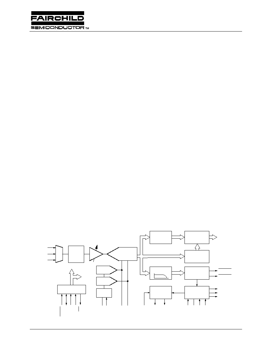
Block Diagram
VIN1
ANALOG
CLAMP
GAIN
D/A
GVSYNC
GHSYNC
PXCK
65-2072-01
LDV
VALID
CVBS7-0
BACK PORCH
CLAMP
DATA
SELECTOR
SUBCARRIER
PHASE-LOCKED
LOOP
SYNC
SEPARATOR
HORIZONTAL
PHASE-LOCKED
LOOP
DIRECT
DIGITAL
SYNTHESIZER
LOWPASS
FILTER
D/A
+1.2V
RESET
SDA
SCL
SA
2-0
INT
COMP
CLK IN
CLK
OUT
DDS
OUT
PFD IN
PXCK SEL
EXT PXCK
C
BYP
V
REF
R
B
R
T
CONTROL
MICROPROCESSOR
INTERFACE
ANALOG INTERFACE
DDS/PIXEL CLOCK INTERFACE
MUX
VIN2
VIN3
A/D
TMC2072
Genlocking Video Digitizer

TMC2072
PRODUCT SPECIFICATION
2
REV. 1.0.4 6/19/01
Functional Description
The TMC2072, a fully integrated self-genlocking video A/D
converter, digitizes NTSC or PAL baseband composite sig-
nals. It accepts video on one of three input channels, adjusts
the gain, clamps to the back porch and digitizes the video at
a user-selectable multiple of the horizontal line frequency.
It extracts horizontal and vertical sync, measures the subcar-
rier frequency and phase, and provides these data with the
digitized composite data over an 8-bit digital video port.
Horizontal and vertical sync outputs are provided, along with
pixel clock (LDV) and twice pixel clock (PXCK).
Operating parameters are set up via a standard two-wire
microprocessor port. The chip can work with either an inter-
nal or an external voltage reference.
Fabricated in an advanced CMOS process, the TMC2072 is
housed in a 100 lead metric quad flat package. Its perfor-
mance is guaranteed from 0 to 70°C and from 4.75 to 5.25
supply volts.
Timing
The TMC2072's A/D converter and digital signal path
operate from alternate cycles of an internally-synthesized
clock, PXCK. This 24.5 to 30 MHz clock is derived from the
incoming 20 MHz reference clock and phase-locked to the
horizontal sync tips of the incoming analog video stream.
The frequency of PXCK may be set as 1560 (NTSC VGA
square pixel), 1716 (NTSC D1), 1732 (PAL D1), or 1888 or
1920 (PAL VGA) times the incoming video line rate.
Timing of the serial microprocessor interface bus is indepen-
dent of the pixel clock and is described under the Micropro-
cessor Interface section that follows Functional Description.
Video Input
Via the microprocessor interface, the user can enable one of
the chip's three analog video input ports. Although each port
normally anticipates a standard video signal level with
286 to 300 mV between sync tip and blank, another control
register bit allows it to be used with half-power (approxi-
mately 70% amplitude) signals. Good crosstalk isolation
accommodates active video on all three inputs simulta-
neously. The user must provide antialias filtering and proper
line termination externally.
Analog Clamp
The front-end analog clamp ensures that the input video falls
within the active range of the A/D converter. The digitized
composite video output can be clamped to the back porch by
a secondary digital clamp.
Automatic Gain Adjustment
To accommodate approximately a ±15% range in video
signal amplitudes, the TMC2072's on-chip AGC circuit
engages for one video frame following either: 1) initial lock
after reset; 2) loss and recovery of lock while operating; or
3) setting of control bit AGCEN high by the host micropro-
cessor. The AGC operation adjusts the A/D converter's on-
chip reference voltages until video blank causes it to output
approximately 1/4 of its full range. The chip then holds this
gain adjustment constant until a new AGC sequence is initi-
ated by AGCEN going high or by loss and recovery of video
lock. The one-frame timeout prevents the gain control from
riding gain and trying to track noise or minor variations in
signal strength.
To handle doubly-terminated and other weak video signals,
the user should set the VGAIN control bit high, thereby
boosting video gain 50% above nominal.
Analog-to-Digital Converter
The TMC2072 contains a high-performance 8-bit A/D
converter. Its gain and offset are automatically set as a part of
the automatic gain adjustment process during initial signal
acquisition, and require no user attention.
The reference voltages to the A/D converter are set up by
internal D/A converters under automatic control during
genlock acquisition. These voltages determine the gain and
offset of the A/D converter with respect to the video level
presented at its input.
Low-Pass Filter
The digitized composite video stream is digitally low-pass
filtered to remove chrominance components from the sync
separator. Filtering provides robust operation by optimizing
the signal-to-noise ratio of the synchronizing/blanking por-
tion of the video, improving the accuracy of the back porch
blanking level detector.
A digital sync separator provides the output sync signals,
GHSYNC and GVSYNC, and times internal operations.
Horizontal Phase-Locked Loop
A phase-locked loop generates PXCK, at twice the pixel
rate. The reference signal for the horizontal phase-locked
loop is generated by the Direct Digital Synthesizer (DDS).
The DDS output is constructed with an internal D/A con-
verter and is output from the TMC2072 via the DDS OUT
pin. This signal is passed through an external LC filter and
input to the horizontal phase-comparator.
The frequency of the DDS output is one ninth of that of
PXCK.
A 20MHz clock is required to drive the DDS. Preferably, this
may be input to the TMC2072 via CMOS levels on the CLK
IN pin. Alternately, a 20MHz crystal may be directly
connected between CLK IN and CLK OUT with tuning
capacitors to activate the internal crystal oscillator circuitry.
PRODUCT SPECIFICATION
TMC2072
REV. 1.0.4 6/19/01
3
If incoming video is lost or disconnected after the TMC2072
has locked to it, PXCK and GRS data will continue, but
GVSYNC and every eighth GHSYNC will cease until lock
is reestablished. The GRS will report the initial subcarrier
frequency set by the Format select bits of the Control
Register. The TMC2072 will relock to incoming video
within two frames after it is restored.
Subcarrier Phase-Locked Loop
A fully-digital phase-locked loop is used to extract the phase
and frequency of the incoming color burst. These frequency
and phase values are output over the CVBS bus during the
horizontal sync period. Fairchild's video decoder and gen-
lockable encoder chips will accept these data directly.
Back Porch Digital Clamp
A digital back-porch clamp is employed to ensure a constant
blanking level. It digitally offsets the data from the A/D con-
verter to set the back porch level to precisely 3C
h
for NTSC
and 40
h
for PAL. When the digital clamp is enabled, the
CVBS video output data is the A/D conversion result minus
the back porch level plus 3C
h
(40
h
for PAL). The back-porch
level is low-pass filtered to minimize streaking artifacts from
subtle line-to-line variations.
Digitized Video Output
The digitized 8-bit video output is provided over an 8-bit
wide CVBS data port, synchronous with PXCK and LDV.
Subcarrier frequency, subcarrier phase, and Field ID data
(GRS) are transmitted in 4-bit nibbles over CVBS
3-0
during
the horizontal sync tip period at the PXCK rate.
Microprocessor Interface
The TMC2072 is controlled by a standard 2-wire bus. Up to
eight TMC2072 devices may be connected to the 2-wire
serial interface with each device having a unique address.
The 2-wire interface comprises a clock input (SCL) and a
bi-directional data (SDA) pin. The TMC2072 acts as a slave
for receiving and transmitting data over the serial interface.
When the serial interface is not active, the logic levels on
SCL and SDA are pulled HIGH by external pull-up resistors.
Data received or transmitted on the SDA line must be stable
for the duration of the positive-going SCL pulse. Data on
SDA must change only when SCL is LOW. If SDA changes
state while SCL is HIGH, the serial interface interprets that
action as a start or stop sequence.
There are five components to serial bus operation:
· Start signal
· Slave address byte
· Base register address byte
· Data byte to read or write
· Stop signal
When the serial interface is inactive (SCL and SDA are
HIGH) communications are initiated by sending a start sig-
nal. The start signal is a HIGH-to-LOW transition on SDA
while SCL is HIGH. This signal alerts all slaved devices that
a data transfer sequence is coming.
The first eight bits of data transferred after a start signal com-
prise a seven bit slave address and a single R/W bit. The R/W
bit indicates the direction of data transfer, read from or write
to the slave device. If the transmitted slave address matches
the address of the device (set by the state of the SA2:0 input
pins.), the TMC2072 acknowledges by bringing SDA LOW
on the 9th SCL pulse. If the addresses do not match, the
TMC2072 does not acknowledge.
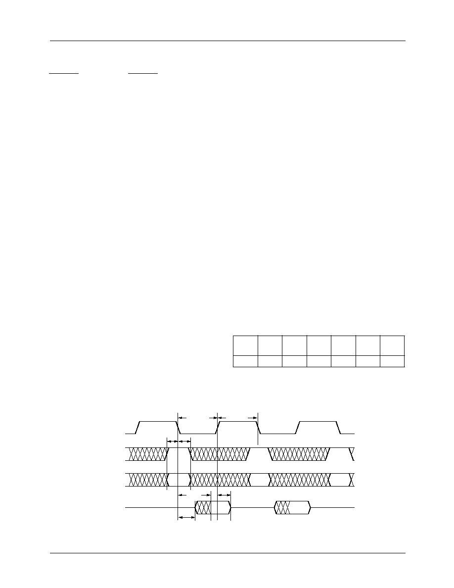
Table 1. Serial Port Addresses
The address is 1000 SA
2
SA
1
SA
0
.
A
6
A
5
A
4
A
3
A
2
(SA
2
)
A
1
(SA
1
)
A
0
(SA
0
)
1
0
0
0
1/0
1/0
1/0
Figure 1. Microprocessor Parallel Port Read Timing
t
PWLCS
t
PWHCS
t
SA
t
HA
SCL
SDA
SA
2
SA
0
D
7
D
0
t
DOM
t
DOM
t
DOZ
65-2072-02
TMC2072
PRODUCT SPECIFICATION
4
REV. 1.0.4 6/19/01
Data Transfer via Serial Interface
For each byte of data read or written, the MSB is the first bit
of the sequence.
If the TMC2072 does not acknowledge the master device
during a write sequence, the SDA remains HIGH so the mas-
ter can generate a stop signal. If the master device does not
acknowledge the TMC2072 during a read sequence, the
TMC2072 interprets this as "end of data." The SDA remains
HIGH so the master can generate a stop signal.
Writing data to specific control registers of the TMC2072
requires that the 8-bit address of the control register of inter-
est be written after the slave address has been established.
This control register address is the base address for subse-
quent write operations. The base address autoincrements by
one for each byte of data written after the data byte intended
for the base address. If more bytes are transferred than there
are available addresses, the address will not increment and
remain at its maximum value of 10h. Any base address
higher than 10h will not produce an ACKnowledge signal.
If no ACKnowledge is received from the master, the encoder
will automatically stop sending data.
Data are read from the control registers of the TMC2072 in
a similar manner. Reading requires two data transfer
operations:
The base address must be written with the R/W bit of the
slave address byte LOW to set up a sequential read
operation.
Reading (the R/W bit of the slave address byte HIGH)
begins at the previously established base address. The
address of the read register autoincrements after each byte is
transferred.
To terminate a read/write sequence to the TMC2072, a stop
signal must be sent. A stop signal comprises a LOW-to-
HIGH transition of SDA while SCL is HIGH.
A repeated start signal occurs when the master device driv-
ing the serial interface generates a start signal without first
generating a stop signal to terminate the current communica-
tion. This is used to change the mode of communication
(read, write) between the slave and master without releasing
the serial interface lines.
Serial Interface Read/Write Examples
Write to one control register
Start signal
Slave Address byte (R/W bit = LOW)
Base Address byte
Data byte to base address
Stop signal
Write to four consecutive control registers
Start signal
Slave Address byte (R/W bit = LOW)
Base Address byte
Data byte to base address
Data byte to (base address + 1)
Data byte to (base address + 2)
Data byte to (base address + 3)
Stop signal
Read from one control register
Start signal
Slave Address byte (R/W bit = LOW)
Base Address byte
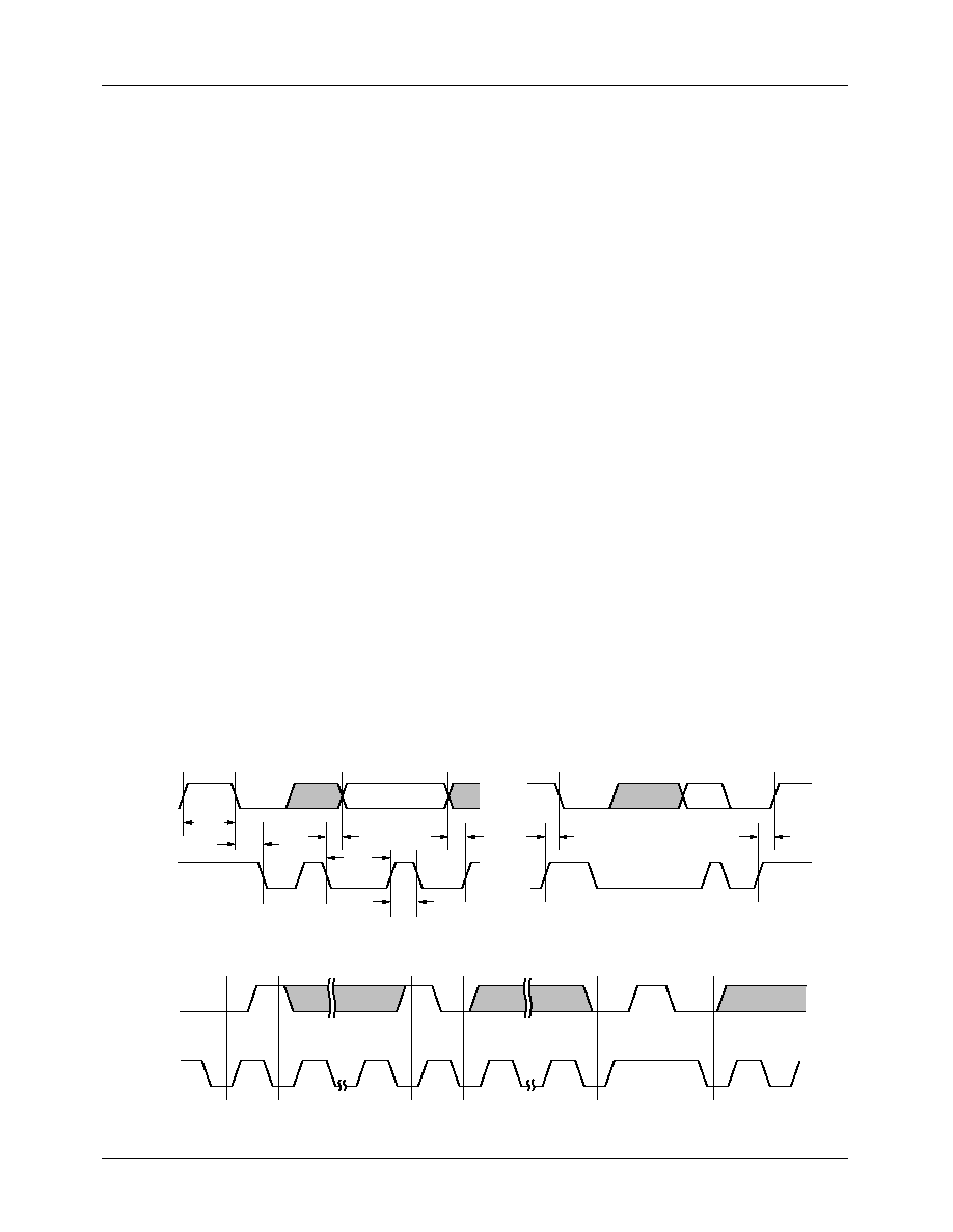
Figure 2. Serial Port Read/Write Timing
Figure 3. Serial Interface Start/Stop Signal
SDA
t
BUFF
t
STAH
t
DHO
t
DAL
t
DSU
t
DAH
t
STASU
t
STOSU
SCL
65-2072-03
STOP
SDA
SCL
START
STOP START
65-2072-04
PRODUCT SPECIFICATION
TMC2072
REV. 1.0.4 6/19/01
5
Stop signal
Start signal
Slave Address byte (R/W bit = HIGH)
Data byte from base address
Stop signal
Read from four consecutive control registers
Start signal
Slave Address byte (R/W bit = LOW)
Base Address byte
Stop signal
Start signal
Slave Address byte (R/W bit = HIGH)
Data byte from base address
Data byte from (base address + 1)
Data byte from (base address + 2)
Data byte from (base address + 3)
Stop signal
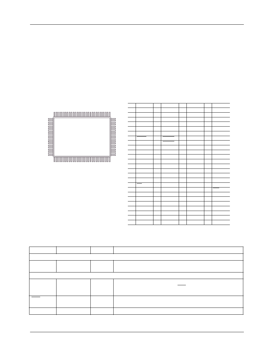
Pin Assignments
Pin Definitions
Pin Name
Pin Number
Pin Type
Function
Video Input
V
IN1-3
65, 61, 58
1.23Vp-p
Composite Video Input. Video inputs,1.235 Volts peak-to-peak,
sync tip to peak color
Clocks
CLK IN
91
CMOS
20 MHz DDS clock input. 20 MHz CMOS clock input to DDS. This
pin may also be used along with CLK OUT for directly connecting
crystals.
CLK OUT
93
CMOS
Inverted clock output. Inverted DDS clock output. This pin may
also be used along with CLK IN for directly connecting a crystal.
PXCK
45
CMOS
2x Pixel clock output. 2x oversampled line-locked clock output.
65-2072-05
SA
0
SA
1
SA
2
SDA
SCL
V
DD
RESET
D
GND
NC
NC
NC
NC
NC
NC
NC
D
GND
INT
V
DD
NC
NC
CVBS
0
CVBS
1
CVBS
2
CVBS
3
CVBS
4
1
2
3
4
5
6
7
8
9
10
11
12
13
14
15
16
17
18
19
20
21
22
23
24
25
1
30
31
50
51
80
100
81
V
DD
D
GND
CVBS
5
CVBS
6
CVBS
7
BURL
GHSYNC
GVSYNC
VALID
FID0
FID1
NC
D
GND
D
GND
LDV
D
GND
V
DD
NC
V
DD
PXCK
D
GND
D
GND
V
DD
V
DDA
A
GND
26
27
28
29
30
31
32
33
34
35
36
37
38
39
40
41
42
43
44
45
46
47
48
49
50
Pin Name
Pin Name
V
DDA
V
DDA
NC
NC
A
GND
NC
R
B
V
IN3
NC
V
DDA
V
IN2
NC
A
GND
V
DDA
V
IN1
NC
A
GND
R
T
A
GND
V
REF
NC
A
GND
V
DDA
A
GND
C
BYP
51
52
53
54
55
56
57
58
59
60
61
62
63
64
65
66
67
68
69
70
71
72
73
74
75
NC
PFD IN
NC
NC
NC
A
GND
DDS OUT
NC
NC
NC
PXCK SEL
V
DDA
COMP
A
GND
D
GND
CLK IN
V
DD
CLK OUT
EXT PXCK
D
GND
D
GND
D
GND
V
DD
NC
V
DD
76
77
78
79
80
81
82
83
84
85
86
87
88
89
90
91
92
93
94
95
96
97
98
99
100
Pin Name
Pin Name
Note:
1. NC = No internal connection between package
and IC. Fairchild Semiconductor recommends
leaving these pins open to simplify board
upgrades to potential future genlock chips.